Helen Frankenthaler PCB Circuit Board R&D Center

alumina ceramic pcb 0.5

DPC alumina ceramic PCB manufacturer – Topright Circuits PCB and PCB Assembly

DPC alumina ceramic PCB manufacturer – Topright Circuits PCB and PCB Assembly

Topright Circuits PCB and PCB Assembly

Ceramic PCB

DPC alumina ceramic PCB manufacturer

Product Specifications
  • layer : 1 layer
  • Size : 34*33mm
  • board thickness : 0.635mm
  • copper thickness : 35UM
  • material : Alumina PCB (Al2O3 PCB)
  • Surface treatment : ENIG 1.3U”
  • DPC process
Ceramic PCB Process Capability
ProjectThick film ceramic board process capabilitiesDBC/DCB Copper Copy Ceramics Square Process CapabilityDPC direct copper plating ceramic substrate process capacityAMB activated metal welding ceramic substrate
Number of circuit layers10 layer2 layer2 layer2 layer
Biggest size200*200mm138*178mm138*190mm114*114mm
Minimum board thickness0.25mm0.30mm~0.40mm0.25mm0.25mm
Maximum board thickness2.0mm1L: 1.3mm; 2L: 1.6mm2.0mm1.8mm
Conductor thickness5um-13um3.9oz-8.6oz2um-200um8oz-22.9oz
Minimum line width/line distance6/8mil (0.15/0.20mm)12/12mil (0.30/0.30mm)6/8mil (0.15/0.20mm)20/20mil (0.50/0.50mm)
SubstrateOne aluminum, aluminum nitride, oxidation, oxideAlumina, aluminum nitride, oxideAlumina, aluminum nitride, oxide, silicon nitrideAluminum nitride, silicon nitride
Base material0.25, 0.38, 0.50, 0.635, 0.80, 1.0, 1.25, 1.5, 2.0mm0.25, 0.38, 0.50, 0.635, 0.76, 1.0mm0.25, 0.38, 0.50, 0.635, 0.80, 1.0, 1.25, 1.5, 2.0mm0.25, 0.38, 0.50, 0.635, 0.76, 1.0mm
Minimum4mil (0.1mm)
Minimum hole distanceNPTH: 16mil (0.30mm); PTH: 20mil (0.5mm)
Minimum PAD ring (single)6mil(0.15mm)N/A3mil(0.075mm)N/A
PTH minimum hole wall copper thickness4mil(10um)N/A4mil (10um)N/A
Welding pad minor diameter10mil(0.25mm)8mil(0.20mm)6mil(0.15mm)8mil(0.20mm)
Group welding bridge12mil(0.30mm)8mil(0.20mm)6mil(0.15mm)8mil(0.20mm)
BGA pads minimum spacing12mil(0.30mm)8mil(0.20mm)5mil(0.125mm)8mil(0.20mm)
PTH/NPTH pore diameter tolerancePTH: ±4mil (0.1mm) ; NPTH: ±2mil (0.05mm)
Pole bias tolerance± 4mil (0.1mm)
ToleranceLaser cutting: +0.2/0.05mm; Mold type type: +0.25/0.20mmLaser cutting: +0.2/0.05mmLaser cutting: +0.2/0.05mm; Mold type type: +0.25/0.20mmLaser cutting: +0.2/0.05mm
Line width/line distance tolerance± 5mil (0.125mm)± 5mil (0.125mm)± 1mil (0.025mm)± 5mil (0.125mm)
Surface treatmentAgPd, AuPd, Mn/NiOSP ,ENIG, ENEPIG etcOSP,ENIG,ENEPIG etcOSP ,ENIG,ENEPIG etc
Thermal Stress1 hour @ 350℃3 x 10 Sec @ 280 ℃15 min @ 350 ℃3 x 10 Sec @ 280 ℃
FAQ

Q1: What’s your minimum order quantity?

A1: We have no MOQ ,1pcs is welcomed.

Q2:What file we should offer?

A2: PCB:Gerber file is better, ( Protel, power pcb, PADs file), PCBA: Gerber file and BOM list.

Q3: No PCB file/GBR file, only have the PCB sample, can you produce it for me?

A3: Yes, we could help you to clone the PCB. Just send the sample PCB to us, we could clone the PCB design and work out it.

Q4: What any other information should be offered except for file?

A4:Following specifications are needed for quotation: a) Base material b) Board thickness: c) Copper thickness d) Surface treatment: e) color of solder mask and silkscreen f) Quantity

Q5:I am very satisfied after I read your information, how can I start to purchase my order?

A5: You could send your file to requirements to our email : pcb@frankenthalerfoundation.org

Q6 : What’s your payment type ?

A6: TT , Western Union , Paypal , Alipay etc

Q7: What is delivery terms and time?

A7: We usually use FOB terms and ship the PCBs in 5-15 workdays depending on your order quantity.

Q8: What is your packaging and shipment type ?

A8:

Related Products

Multilayer 8 layers impedance control PCB circuit board with red solder mask

6 layers high frequency PCB board ,roger and fr4 mixed material pcb

Multilayer HDI PCB circuit board with Blind buried hole

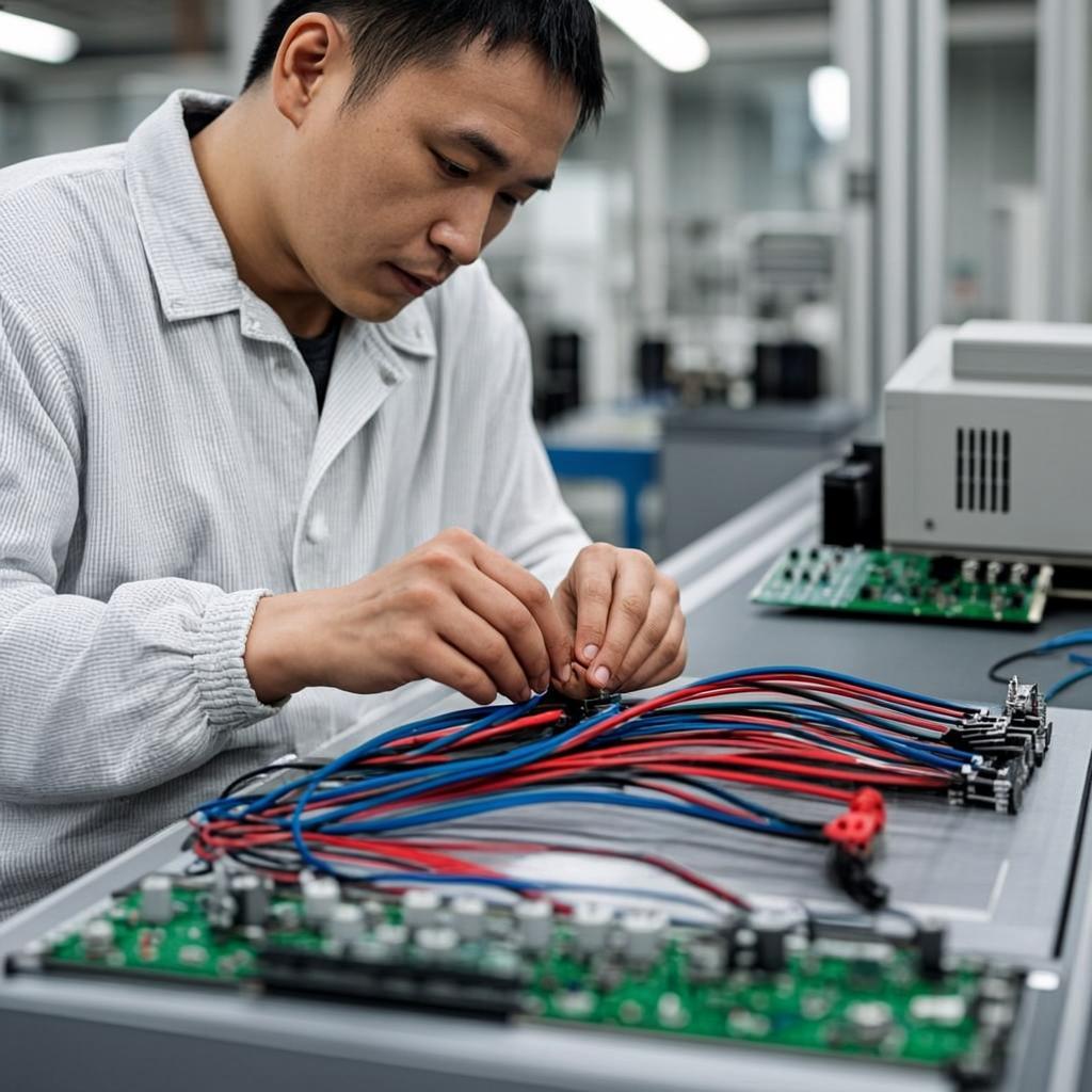
Provide one-stop PCB&PCBA solution for you

Products
  • PCB Assembly
  • Fr4 PCB
  • Flexible PCB
  • Rigid-flexible PCB
  • Rogers PCB
Products
  • Taconic PCB
  • Ceramic PCB
  • Copper PCB
  • Aluminum PCB
  • Special PCB
Contact us
  • +8615919758327
  • Whatsapp : +8615919758327
  • pcb@frankenthalerfoundation.org
  • pcb@frankenthalerfoundation.org
  • ShangXing West Industry park ,Shajing Street ,Baoan, Shenzhen,Guangdong,China

© Copyright 2015.Topright Circuits All Rights Reserved

  • Home
  • Product
  • About Us
  • PCB&PCBA Knowledge
  • Contact