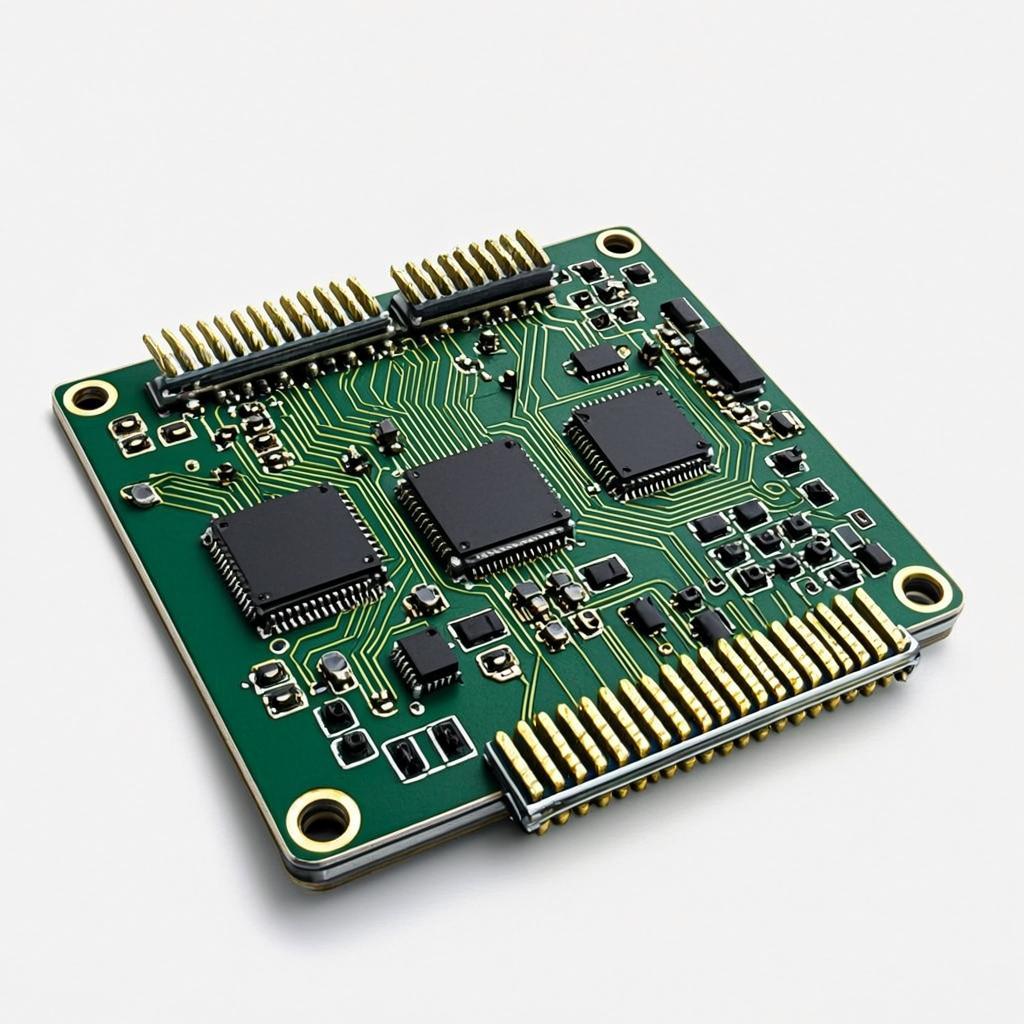
Aluminum-Nitride PCB (AIN PCB)
Many users of PCBs (Printed Circuit Boards) find that ceramic PCBs offer significant advantages over traditional boards made from materials such as fiberglass or epoxy resin. The key benefits come from the use of ceramic substrates, which provide high thermal conductivity and a low coefficient of thermal expansion (CTE)—critical factors for improving reliability and performance in electronic circuits.
A ceramic PCB is extremely versatile and can often replace an entire traditional PCB with a simpler design and enhanced performance. These boards are widely used in high-power circuits, chip-on-board (COB) modules, LED lighting systems, and proximity sensors, where efficient heat dissipation and stability are essential.
In simple terms, a ceramic printed circuit board is a type of PCB that uses a ceramic material base or substrate—usually an inorganic dielectric—rather than the conventional fiberglass or epoxy resin base. It consists of a thin, insulating layer of ceramic combined with a conductive metal layer, delivering superior thermal management, electrical insulation, and mechanical strength for demanding electronic applications.
In addition to their excellent thermal conductivity and low coefficient of thermal expansion (CTE), ceramic PCBs provide several other advantages that make them ideal for high-performance electronics.
Key benefits include:
Ceramic PCBs are typically built with ceramic cores, with Aluminum Nitride (AlN) and Alumina (Al₂O₃) being the two most widely used materials. Both types deliver superior thermal performance compared to metal-core PCBs, since they do not require an additional dielectric layer between the core and the circuits.
For applications requiring superior heat dissipation,Aluminum Nitride PCBs are the ideal choice, with thermal conductivity greater than 150 W/m·K. However, because AlN is more expensive, many companies opt for Aluminum Oxide (Alumina) PCBs, which offer 18–36 W/m·K while still outperforming metal-core PCBs.
Both materials eliminate the need for an electric layer between the core and the circuits, improving thermal performance. Additionally,ceramic PCBs can be manufactured with gold plating on exposed pads to prevent silver corrosion in high-sulfur environments.
While Aluminum Nitride and Alumina are the most common, other advanced ceramic materials can also be used for PCB manufacturing:
Due to high operating temperatures, ceramic PCBs are typically not finished with OSP, HASL, or Pb-free HASL. Instead, they are often coated with:
These finishes protect exposed pads and reduce the risk of silver corrosion, particularly in harsh or sulfur-rich environments.
The leading reason industries turn to ceramic PCBs is their exceptional thermal conductivity. This property gives ceramics a clear edge over traditional PCB materials like FR4 and metal-core substrates. Combined with better CTE matching and hermetic sealing, ceramics ensure long-term reliability in demanding applications.
However, ceramic substrates and boards are significantly more expensive than traditional PCB materials. For high-volume production, costs can accumulate, but for companies requiring high-power, high-frequency, and thermally demanding performance, ceramic PCBs are often the only viable solution.
The exact level ofthermal conductivityin a ceramic PCB depends on themanufacturing process, grain size, and material composition. While values may vary, industry experts generally provide the following ranges:
During inspection, several issues were identified with the received substrates that must be addressed before approval for production:
During Scanning Electron Microscope (SEM) inspection, the following observations were recorded:
Additional defects were observed on the surface of the Gold (Au) layer: