Article
2 November 2021
and
1 Department of Sustainability Science, School of Energy Systems, Lappeenranta-Lahti University of Technology LUT, P.O. Box 20, 53851 Lappeenranta, Finland
2 Department of Mechanical Engineering, School of Energy Systems, Lappeenranta-Lahti University of Technology LUT, P.O. Box 20, 53851 Lappeenranta, Finland
* Author to whom correspondence should be addressed.
This article investigates the potential environmental impacts of four-layer printed circuit board (PCB) production from cradle to grave. The study starts with a lifecycle assessment of conventional PCB production. Then, the alternative materials of polyethylene terephthalate (PET), polylactic acid (PLA)/glass fiber composite and paper are investigated for the substrate. A conventional PCB adopts copper as the conductive material and requires an etching process. The environmental impacts of changing the conductive deposition method to an additive method by printing silver nanoparticles is studied. In a conventional PCB, electricity generation contributes 41% of the global warming potential (GWP) and 38% of the abiotic resource depletion (ADP), in the fossil category. By applying an additive manufacturing method, the GWP of PCB manufacturing can be reduced to 14% of that of the conventional method. A sensitivity analysis of silver recycling illustrates that a 40% higher silver recycling rate would decrease the GWP of silver material by about 48–60%. Uncertainty in the energy consumption of PCB production would alter the environmental impacts; however, even with the most conservative energy consumption in a conventional PCB production method, the environmental impacts of the additive method are about five times lower than those of conventional PCB production.
By 2021, the market for the Internet of Things (IoT) has been forecast to expand to billions of devices [1], which will consequently produce a considerable amount of electronic waste. One requirement of digitalization is that electronics are embedded in products, which, at some point in their lifecycle, may be released into the natural environment. Examples of applications for embedded electronics include sensors in disposable smart packaging, flexible and printable electronics embedded in consumer products, health care products and disposable sensors for weather and crop monitoring. On the other hand, the increasing amount of electronic equipment increases the environmental impacts of their materials and production.
New trends and applications in the electronic industry require novel developments and the re-designing of sustainable alternatives to the existing production stream. This new market opens a discussion on how conventional practices in electronics manufacturing are in accordance with the sustainability principles and how the environment may benefit from the transformation of production practices in the electronics industry.
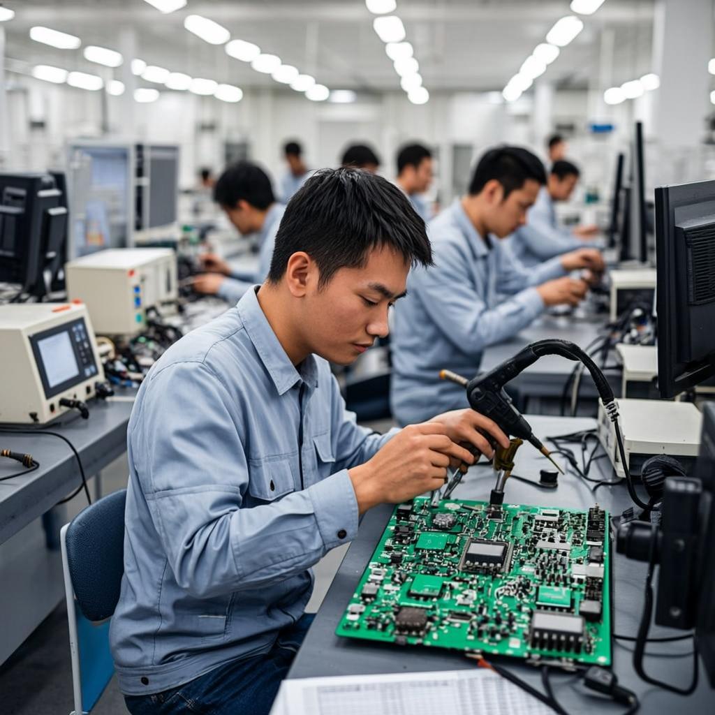
Printed circuit boards (PCBs) are a fundamental component in almost all electronic products, and circuits, devices and chips are built on PCBs. Conventional multilayer PCBs consist of a core dielectric layer (substrate) clad with copper as a conductive material on both sides and laminated with several layers of prepreg and copper foil by applying a high pressure and temperature [2]. Chemical resists with printed circuit patterns are deposited on the conductive layer. The copper surface is exposed to chemicals and the extra copper is removed by chemical etching [3].
The substrate of PCB, most commonly known as flame retardant (FR4), is a composite material consisting of three main components: epoxy resin, woven glass fiber (GF) and copper foil [3]. Epoxy resin is derived from non-renewable crude oil. The manufacturing process of GF is energy-intensive, and the copper preparation method requires the use of extensive energy and solvents [4].
Bio-based materials, as a substrate of consumer electronics, could embrace the requirements of embedded electronics such as being flexible, lightweight, printable and low-cost, while enhancing the environmental profile of these products by incorporating biodegradability and composability, and decreasing the energy and materials used in their production. The utilization of flexible and bio-based composites to produce PCB substrates has led many researchers to study the feasibility of eco-friendly alternative substrates. The authors of [2] investigated the application of lignin incorporated into a brominated epoxy matrix. The authors of [5] studied the application of epoxidized linseed oil obtained from flax plants, combined with a small portion of conventional epoxy resin (bisphenol-F). The authors of [6] investigated the environmental impacts of paper-based multilayer PCB. The authors of [7] utilized polylactic acid (PLA) as the substrate of PCB. The authors of [8] investigated the utilization of polyethylene terephthalate (PET) as the substrate of flexible PCB. However, there is a lack of studies on the environmental impacts of the new generation of printed and flexible PCBs on substrates such as PET and PLA composites. PLA is produced from pure renewable materials, such as corn and sugar beets [9], and is considered a biodegradable polymer for developing sustainable and environmentally friendly electronics [7]. PLA is mostly applied in food packaging at present, either as a bottle for liquids [10] or as a thin film [11]. There are few scientific articles regarding the fabrication of electronic devices on PLA substrates, since the glass transition temperature of PLA is very low (Tg = 58 °C), which implies significant constraints on the manufacturing of electronics, where the substrate is usually exposed to higher temperatures [12,13,14].
The improvement of the mechanical and thermal properties of PLA has attracted the attention of many researchers. The main cause of the poor mechanical and thermal performance of PLA is PLA’s poor crystallization abilities [15]. Glass fiber is the most common synthetic material utilized to reinforce polymers, due to its excellent mechanical and heat-resistance performance [16].
Electrically conductive adhesives (ECAs) have been widely applied in electronic research and development and the functionalities of ECA for applications on paper, PET and PLA have been proven [17]. There are several possible options for the conductive ink used for PCBs. The goal of this study was not to compare different conductive inks. AgNP was selected as the ink, since experimental results from the literature and other studies in the ongoing research project showed the feasibility of using AgNP as the printing ink [18,19,20,21]. This study adopted silver nanoparticles (Ag NPs) and thermoset polyurethane as the ECA and screen printing as the deposition method.
Material recovery from disposed PCBs is an important issue since old PCBs contain valuable materials and may endanger the environment if they are not managed properly. Thus, several recycling and recovery processes have been developed to close the loop in PCB production [22]. A sensitivity analysis of silver recovery is included in this study to examine the importance of proper waste treatment.
The aim of the current study is to fill the literature gap of a cradle-to-grave lifecycle assessment (LCA) to assess and compare the environmental impacts of a novel trend in the green and flexible electronic industry. The current article quantifies the environmental impacts of PCB production and demonstrates the benefit of moving from subtractive manufacturing to additive manufacturing.
The current article is part of the ECOtronics project, in which different research units investigate the electrical circuits, material behavior and commercial aspects of developing printed electronics. The objective of this study is to demonstrate the potential of printed electronics to decrease the environmental impacts throughout the products’ lifecycle. The scenarios in this article were based on the best commercially available materials and could help electronic circuit designers to understand the environmental profile of their products.
The data used to conduct a lifecycle assessment were gathered by searching through the following sources:
A lifecycle assessment (LCA) quantifies the potential environmental impacts throughout the products’ lifecycle [23]. The LCA framework is implemented in four phases: goal and scope definition, lifecycle inventory (LCI), lifecycle impact assessment (LCIA) and interpretation. In addition, a sensitivity analysis is recommended to enhance the creditability of the LCA study [23].
The goal of this LCA study was to assess and compare the environmental impact of alternative production methods and materials for PCB manufacturing. The conventional substrate in this study refers to fiber-glass-reinforced brominated epoxy resin (FR4) and the comparative cases are PET, PLA/GF composite and paper. The conductive material in the baseline is copper and, in other cases, the baseline is an electrically conductive adhesive, which is a combination of 50% resin and 50% silver nanoparticles.
The manufacturing method for the baseline scenario is conventional copper treatment (chemical etching is involved), and, in the other cases, the method is lab-scale PCB production, which is mainly based on the experimental procedure described in [6].
The functional unit in this LCA study was set as one m 2 of four-layer PCB. The thickness of the conventional PCB substrate is 1.6 mm, whereas, for the alternative cases, the thickness of the substrate material was retrieved from [8], which has two layers of 125 µm and one layer of 36 µm.
The system boundary of this study is depicted in [Figure 1], covering cradle-to-grave processes. It includes the raw material acquisition, manufacturing, and waste disposal of PCB. Transport and use phases are excluded from the system boundaries because they are assumed to be the same for all alternatives. Most of the utilized data represent global conditions; however, due to the lack of global data, some data sources correspond to more specific geographical locations.
Several possible alternative materials were studied for the PCB substrate. PET, PLA/GF and paper were selected in this study, and etched copper was substituted with ECA containing silver nanoparticles (Ag NPs). Five study scenarios are listed in [Table 1].
S1 represents the baseline scenario for a conventional FR4-based PCB, and S2 is a hypothetical scenario designed to check the environmental impacts when only the conductive material is changed to Ag NPs. The intention of introducing S2 was to demonstrate the environmental benefits when only the manufacturing process (not the substrate material) is changed from a subtractive method to an additive method. Then, in scenarios S3, S4 and S5, the substrate material is also changed. In S2–S5, Ag NPs were utilized as the conductive material, deposited on the substrate using the screen-printing method. S3 represents a scenario related to the PET-based substrate. S4 depicts the scenario derived from the PLA/GF composite. The substrate material in scenario S5 is normal printing paper.
From the functional perspective, the function of S3, S4 and S5 is, to some extent, different; PET plastic is applicable, whereas a transparent substrate is needed. PLA/GF is a bio-compostable plastic and would be used in bioplastic packaging. Using paper as the substrate has the advantage of biodegradability and is suitable in paper and cardboard packaging. The objective of this article was not to compare different substrate materials, but to show the environmental impacts of moving toward sustainable electronics.
LCI is an LCA stage quantifying the inputs and outputs of the studied system, and is performed for each scenario. [Table 2] shows the data source for each unit process. The LCIs for processes in Scenarios 1 and 2 were mainly obtained from the Ecoinvent 3.6 database, with the activity name “printed wiring board production, for surface mounting, Pb free surface”. This process represents the manufacturing of 1 m 2 of a six-layer PCB based on the FR4 substrate. The dataset was compiled using the data collected during 2003–2006 from environmental reports of three PCB manufacturers in Europe and it covers the manufacturing processes of a printed wiring (circuit) board: raw materials, energy consumption, emission to air and water and waste amount from the production of 1 m 2 of PCB [24].
The literature has reported controversial results regarding the electricity and heat consumption involved in the manufacturing of conventional FR4-based PCBs (S1 and S2). The electricity and heat consumption values in the Ecoinvent database for a six-layer PCB are 326 and 105 kWh. The authors in [6] collected the inventory data from a manufacturing plant in China and reported a total energy consumption for the manufacturing process of 20 kWh. The authors in [25] collected the inventory data from a manufacturing plant in Turkey and reported the total energy consumption for the manufacturing process of 1 m 2 of a 2-layer PCB as 7.15 kWh. The authors in [5] reported the energy consumption of a 1 m 2 PCB substrate (only the FR4) as 13.4 kWh. The authors in [26] studied the energy consumption of PCB manufacturing and calculated the energy demand for each unit process of a four-layer PCB production. They reported the total energy demand for the manufacturing of a panel of a 4-layer PCB as about 6 kWh. Considering the typical size of a PCB panel (18 × 24”, 18 × 21”, 21 × 24”) [27], the energy demand for 1 m 2 of a 4-layer PCB would be 18–25 kWh. Therefore, in Scenario 1 of this study, the total energy consumption for manufacturing 1 m 2 of a 4-layer PCB is assumed to be 20 kWh and, in Scenario 2, 10 kWh is taken as the electricity consumption. To assess the impact of