HDI Technology from FlashLineElectronics offers significantly more advantages over more conventional PCB technologies:
Contrary to popular belief that bigger is better, advanced design technologies like via-in-pad offer greater copper areas with fewer layers. As consumers prefer smaller devices, the size of most electronic gadgets like wearables, cameras, and mobiles is shrinking. In fact, consumers are the biggest drivers for the trend towards smaller devices—leading to a shrinking of internal circuits as well. Designers now have the awkward challenge of fitting a greater number of features within a continually shrinking space on the PCB.
As a result, more and more designers are turning to HDI technology for addressing the above transformations. HDI technology helps in making products with significantly more features, but weighing less and being physically smaller. Using much thinner material and miniature components, HDI technology requires the use of special equipment for shrinking the physical size of the board, while expanding the features, speed, and quality of the circuit.
Consumer demand drives the requirements of High-Density Interconnect PCB technology. With HDI Technology combined with multiple via processes allows designers to place a greater number of components on either side of the PCB. These advanced via processes are blind and via-in-pad technologies, and they provide designers with more real estate on the PCB to place components closer together. Add to this the decreasing SMT component sizes and pitches, and the component density on the PCB shoots up tremendously—also helping to reduce signal loss and delays significantly.
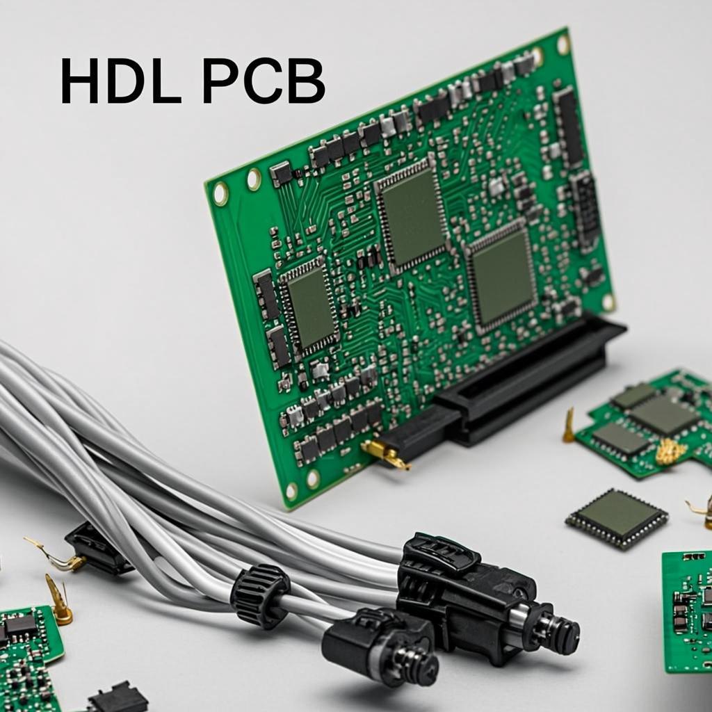
With HDI technology FlashlineElectronics uses various types of micro-vias. This helps increase the real-estate channels available to designers on the PCB for routing traces. Such vias include through vias, buried, and blind micro-vias, landless micro-vias, and micro via-in-pads. FlashLineElectronics uses all filled vias in HDI technology.
Through vias span the entire PCB thickness, beginning from one of the outer layers and ending on the other outer layer. The via may connect intermediate layers as necessary.
These vias start at one intermediate layer and end at another intermediate layer. The via may connect other intermediate layers in between as necessary.
These vias start at one of the outermost layers but finish at one of the intermediate layers, connecting other intermediate layers in between as necessary.
In conventional designs, vias always terminate in pads on both sides. HDI technology allows very small diameter micro-vias, which the designer can place directly on the trace, thus avoiding the necessity of having pads, and resulting in very high-density routing. As these micro-vias are laser drilled, their hole diameter matches the width of the thin traces allowed by HDI technology.
In conventional PCB design, placing vias inside a component’s soldering pad always results in disaster. As conventional vias are unfilled, they wick molten solder away from the pad during reflow, and this causes a dry joint. However, as all micro-vias in HDI technology are epoxy filled, placing micro-vias within the component’s solder pad is not a barrier, as the epoxy prevents solder wicking. Micro-via-in-pad technology allows designers greater freedom with a significant increase in channels while routing traces for fine-pitch components like BGAs.
With HDI technology, FlashLineElectronics uses various fill materials for filling vias. These include conducting and non-conducting epoxy, copper filling, silver filling, and electrochemical fillings. Filled vias have the advantage that they remain buried below a flat copper surface and allow soldering just like normal pads do.
At FlashLineElectronics, we first drill the buried or blind vias and micro-vias. Then we plate and fill them to hide them below the SMT pads. Requiring special equipment, this method is time-consuming, as it requires execution of several drill cycles with good control over the drill depth.
FlashLineElectronics offers a variety of HDI PCB stackups, popular ones being 0-N-0, 1-N-1, and 2-N-2 types.
This HDI PCB type stackup has a laminated core along with a single layer with micro-vias on at least one side. It also has several through vias, if necessary.
This HDI PCB type stackup has a centrally placed laminated core along with a single layer with micro-vias on at least one side. It also has buried micro-vias, and several through vias, if necessary. Designers prefer to stagger the micro-vias and stagger them or stack them in relation to buried micro-vias.
This HDI PCB type stackup has a centrally placed laminated core along with at least two layers with micro-vias on at least one side. It also has blind and buried micro-vias, and some through vias, if necessary. Designers prefer to stagger the micro-vias and stagger them or stack them in relation to buried micro-vias. The type III stackup is the most efficient configuration for large and dense boards containing multiple BGAs with high pin-counts.
At FlashLineElectronics, we make our High-Density Interconnect PCBs very cost effective with proper planning and execution. With our HDI boards, we achieve better results with fewer layers and a smaller sized PCB than what a standard sized PCB offers.