"Thick-copper PCBs, or heavy-copper PCBs, have a copper thickness of more than 2oz. PCBONLINE manufactures PCB copper thickness up to 14 oz."
MATERIALS PCBONLINE uses high-quality sheet materials for heavy copper PCB production. The sheet brand includes Shengyi, Isola, Ventc, etc.
EQUIPMENT The heavy-copper PCB manufacturer PCBONLINE utilizes automatic machines for electrostatic spraying solder masks on thick-copper PCB.
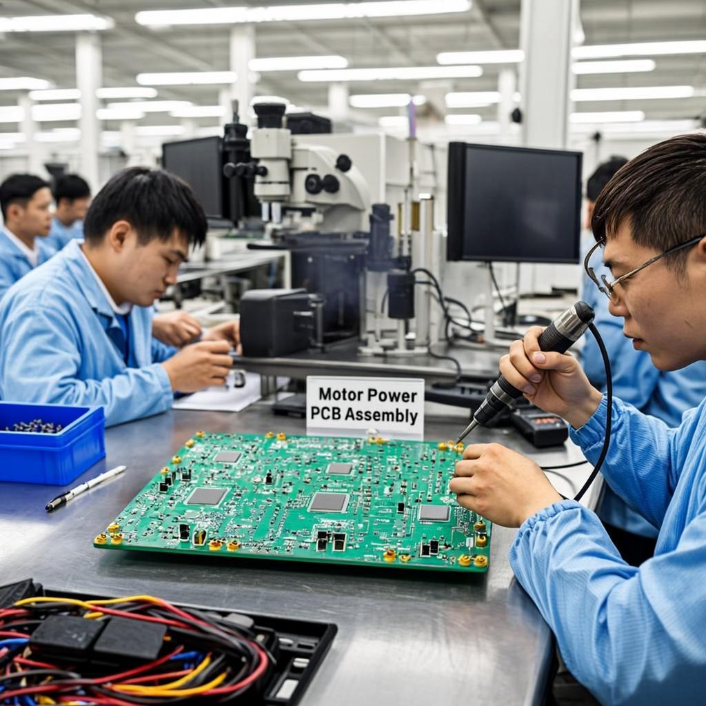
TEAM The professionals from PCBONLINE provide DFM, DFT, DFA, one-on-one engineering support, and PCB manufacturing from proto to bulk production.
QUALITY High-precision circuit etching, small tolerances, uniform ink thickness, best protection effect, and bright appearance of heavy-copper PCB.
CUSTOM PCBONLINE manufactures and assembles many types of custom heavy-copper PCBs with a copper thickness range from 3oz to 14oz.
TRANSPORT PCBONLINE provides various thick-copper PCB shipping methods, including air, sea, and rail shipping by DHL, FedEx, and UPS.
A heavy-copper PCB, or thick-copper PCB, is a printed circuit board with a copper thickness of more than 2oz.
Heavy-copper PCBs are used in applications that pass high currents. Aluminum PCBs and OSP PCBs can't be made to be thick-copper PCBs.
Typically, heavy copper PCBs have at most 8 PCB layers, and the circuit is relatively simple.
If a PCB has a large PCB copper thickness, such as 4oz, 8oz, and even 14oz, it can withstand a large electricity current to pass through. But remember that the trace space/width of heavy-copper PCB should be large.
At the heavy-copper PCB manufacturer PCBONLINE, the copper thickness range of heavy-copper PCBs falls from 3oz to 14oz. And the thick-copper PCB can have the substrate materials of FR4, PI, PET, and copper.
For heavy-copper PCB manufacturing, PCBONLINE uses the electrostatic spray solder mask process to replace the traditional solder mask printing.
The reason why PCBONLINE does not use traditional solder mask printing on thick copper PCBs is that it causes oil to accumulate in the corners of the circuit traces and holes.
Meanwhile, the ink will be very thin in the non-copper areas, and the overall surface of the board is ununiform. When high-current passes through the PCB, electric breakdown may happen at the thinner solder mask areas.
The electrostatic spray solder mask is used for heavy-copper PCB manufacturing because it directly and evenly sprays on the surface of the PCB. And the uniform ink thickness on the entire heavy-copper PCB achieves the best protection and appearance.
Heavy copper PCBs are the first option for large-current systems/devices. Engineers choose heavy copper PCBs for these reasons:
Applications that require flexibility and dense circuitry with compact spaces, such as:
"This is a thick copper multilayer PCB prototype manufactured by PCBONLINE. It has 10 PCB layers. Its has a 10oz PCB copper thickness of both the inner and outer layers."
"The heavyc-copper PCB manufacturer PCBONLINE manufactures the 4oz-copper PCBs for a client. The PCBs demand selective surface finishes, including lead-free HASL and imersion gold."
"Electric vehicle charging pile PCBs usually require 4 to 8 layers, and the copper thickness of the inner and outer layers is about 3oz. So is the case for the heavy-copper PCB in the image."
PCBONLINE has rich experience in thick-copper PCB design, fabrication, and assembly. Read our blogs to explore more details of thick-copper PCBs.