We specialize in delivering robust, high-performance heavy copper PCBs fast. Whether your design requires 4 oz or 10 oz copper builds, our network of advanced fabrication partners can meet your toughest electrical and thermal demands.
Engineers choose San Francisco Circuits for our deep technical expertise, fast turnaround times, and proven ability to deliver complex, high-current boards with unmatched reliability. Our heavy copper solutions are ideal for demanding environments, including mission-critical applications in defense, aerospace, and industrial power systems.
From quick-turn prototypes to full-scale production runs, our team ensures your heavy copper boards are built to perform.
We can turn your heavy copper PCB manufacturing order in as little as 72 hours.
Bareboard Heavy Copper Fabrication
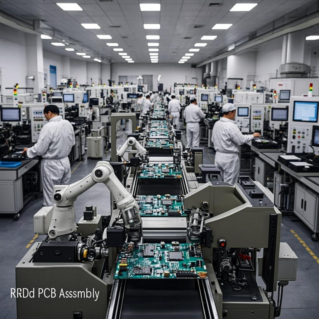
Fab + Assembly (full + partial turnkey)
Call us at 800.SFC.5143 or get an instant PCB quote.
Heavy copper PCBs are generally defined as printed circuit boards that utilize copper weights of at least 3 oz/ft² per layer, significantly more than standard PCB copper thicknesses that are from 0.5 to 3 oz/ft².
Heavy copper PCBs are primarily used to increase current-carrying capacity and enhance thermal management, which is essential for power electronics and other high-demand applications. By increasing copper mass, the board is able to carry high currents with only minimal increases in trace width compared to using lower copper weights.
These boards, also referred to as thick copper PCBs, can be fabricated with copper weights up to 10 oz/ft².
A four-layer PCB with three layers of one-ounce copper with GETEK dielectrics and one of solid 45-oz Cu base.
Heavy copper PCBs are manufactured using four primary methods, each balancing cost, accuracy, and performance.
This high-precision but costly method starts with a very thin copper layer. Heavy copper is built up entirely through plating, then the base layer is etched away. Because this approach often requires 20+ hours of plating, it's reserved for high-performance applications where thicker copper in holes improves current capacity and thermal management. Best for fine-line, high-current designs.
This common method uses a copper layer about half the final desired thickness. Additional copper is plated, then the full thickness is etched. It offers good cost-efficiency, though resolution is lower than the thin-base method. Plated features are more precise than etched ones, and designers must carefully calculate copper buildup in holes.
In this budget-friendly option, a thick copper base is lightly plated and etched. It’s the least expensive but offers limited trace resolution and poor current handling in holes. Typically used in low-tech applications where performance demands are minimal.
Copper thicknesses from 0.020" to 0.040" can be achieved for high-power applications, like Buss Bar replacements. However, extended plating times lead to surface bumps, and imaging through thick photoresist reduces resolution and edge quality. Despite this, the method allows for very robust conductors and high-current paths.
Fabrication of heavy copper boards parallels standard board processes but relies on specialized plating and etching techniques.
Substrate Lamination: Inner layers begin with standard copper foil (0.5 - 2 oz/ft²) laminated onto an FR-4 or alternative substrate. For thick copper, initial copper thickness is often higher to reduce plating time.
The dielectric material may be conventional FR-4 (Tg ~130 °C) or higher-temperature laminates (polyimide, cyanate ester) to tolerate elevated thermal stress.
Copper Plating: Heavy copper features use plating to build up copper thickness on traces, planes, and plated-through holes (PTHs).
Differential etching combines minimal etch back with plating, producing vertical sidewalls and negligible undercut compared to older thick-clad etching methods.
Pattern Etching: After plating, unwanted copper is removed by etching. For thick copper, etch chemistries and tooling are optimized to maintain feature fidelity and to avoid uneven sidewalls.
Heatsink and Thermal Vias: Built-in heatsinks can be electroplated directly onto the board surface, connected via heavy copper thermal vias to internal heat sources. This eliminates the need for post-assembly heatsink attachment and improves overall thermal conductivity.
Heavy Copper PCB
Photo Credit: Robert Tarzwell
Enhanced Current Carrying Capacity
Heavy copper traces allow higher currents through the same footprint compared to standard copper. Inner-layer traces, traditionally de-rated to 50% of outer-layer current capacity, can handle greater loads with heavier copper plating, reducing the risk of thermal failures.
Improved Thermal Management
Thicker copper reduces I²R losses, lowering temperature rise under high current. Integrated heatsinks and copper core layers conduct heat to external dissipation points more efficiently, maintaining stable operating temperatures even in high-power density designs.
Increased Mechanical Strength
Larger copper cross-sections at connector sites and PTHs resist mechanical stresses from vibration and thermal cycling. Heavy copper PTHs provide robustness against cracking under extreme temperature swings (e.g., 25 °C to 260 °C), drastically reducing failure rates during thermal cycle testing.
Space and Cost Optimization
Mixing multiple copper weights on a single layer allows designers to allocate heavy copper only where needed, shrinking board size and reducing layer count. This consolidation can lower material and assembly costs versus stacking parallel 3 oz copper layers to achieve desired current ratings.
Support for Exotic Materials
Heavy copper core PCBs enable designers to exploit high-temperature substrates (e.g., polyimide with Tg ~250 °C) without risking copper crack-outs. Thicker copper in vias and traces mitigates coefficient of thermal expansion mismatches between copper and laminate, extending product life in harsh environments.
By choosing heavy copper PCB materials and construction, engineers mitigate excessive trace widths, minimize voltage drop, and improve heat conduction - capabilities beyond those of standard copper PCBs.
Heavy copper PCB applications span industries where high current, efficient thermal management, and mechanical durability are paramount:
Military and Defense
Aerospace and Avionics
Industrial Power Electronics
Automotive and Transportation
Read more about PCBs for the Automotive Industry.
Telecommunications and Data Centers
Renewable Energy
San Francisco Circuits is a single-source provider for heavy copper PCB fabrication and assembly, offering engineers a streamlined path from prototype to production:
Our engineers have deep experience in heavy copper layouts, including copper core PCBs, copper PCB flex constructions, and assemblies. We can guide customers through selecting the optimal copper weight based on load requirements, thermal margins, and mechanical constraints.
Our speciality lies in quick-turn prototypes ideal for validating heavy copper PCB designs and performing thermal cycle testing, while scaling to production quantities without sacrificing quality.
Beyond bareboard fabrication, SFC offers turnkey PCB assembly, including soldering of power semiconductors and attachment of on-board heatsinks.
Leveraging advanced equipment capabilities and streamlined workflows, we offer aggressive lead times on heavy copper PCB fabrication.