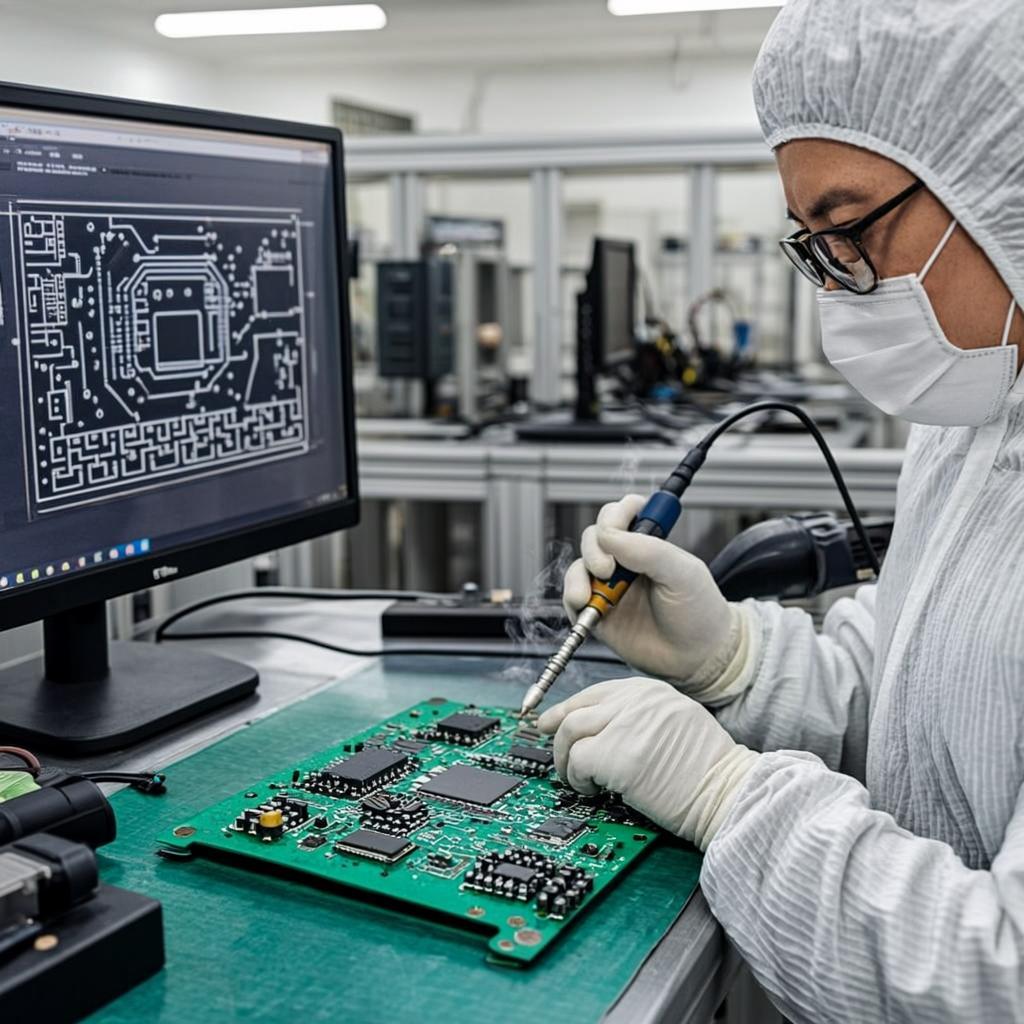
A PCB assembly drawing is a detailed diagram that shows the exact placement, orientation, and identification of all components on a printed circuit board (PCB). Its primary purpose is to guide the assembly process, ensuring that every part is correctly installed during manufacturing. Unlike a PCB layout, which focuses on the routing of traces and electrical connections, or a schematic, which shows the circuit’s functional design, the assembly drawing is specifically designed for production use.
Example:While a schematic might indicate a resistor connects between two points, the assembly drawing shows the resistor’s exact location, rotation, and reference designator on the board. This distinction helps manufacturers translate designs from paper or software into a real, functional PCB.
Accurate assembly drawings are essential for smooth PCB production. They offer several tangible benefits:
Comparison:Consider two PCB assembly drawings for the same board: one detailed and standardized, the other vague and inconsistent. The detailed drawing results in a smooth assembly process, while the vague drawing often leads to errors, delays, and extra costs.
Even experienced engineers can encounter issues when creating assembly drawings. Some frequent challenges include:
Step-by-Step Tip:To avoid these problems, always cross-check component placement against the schematic, verify mechanical details, and apply standardized symbols consistently.
Proper component placement and orientation is crucial to ensure the PCB functions correctly and can be efficiently assembled.
Step-by-Step Guidelines:
Example:A reversed LED or electrolytic capacitor can cause circuit failure. In contrast, a clearly marked assembly drawing ensures the component is installed correctly the first time.
Integrating the BOM with the assembly drawing streamlines manufacturing and reduces errors.
Best Practices:
Comparison:
Mechanical information ensures the board fits correctly in its enclosure and avoids conflicts during assembly.
Key Elements to Include:
Step-by-Step Annotation:
Example:A missing keep-out area can result in a tall capacitor colliding with the case, requiring costly rework.
Clear silkscreen and layer markings are essential for efficient assembly and inspection.
Tips:
Best Practices Example:
Following industry standards ensures that PCB assembly drawings are clear, consistent, and compatible with manufacturing processes.
IPC-2612:Defines the standard format and content for PCB assembly drawings. It covers component placement, reference designators, and layer information.
IPC-2581B:A standardized, machine-readable format for exchanging PCB design, fabrication, and assembly data, enhancing automation, reducing errors, and supporting complex board types such as HDI and rigid-flex PCBs.
Benefits:
Example:A PCB assembly drawing following IPC-2612 clearly shows pin 1 orientation, component designators, and layer information, making it easier for any assembler to work without confusion.
Using consistent symbols and annotations avoids misinterpretation and ensures accurate assembly.
Step-by-Step Guide:
Example:Marking all polarized capacitors with a plus (+) sign and consistent orientation arrows reduces the risk of reverse installation.
Accurate dimensioning and tolerances help ensure components fit precisely and function reliably.
Clearly indicate acceptable placement deviations for each component. Include tolerances for X, Y positions and rotation angles when needed.
Step-by-Step Tips:
Example:
Benefit:Proper dimensioning ensures all components are installed correctly, reduces rework, and improves overall product quality.
Using layer colors and markings effectively improves readability and reduces assembly errors.
Recommended Color Codes:
Examples:Highlight high-current traces, power nets, or critical components using bright or contrasting colors. This makes them stand out for assemblers and inspectors.
Benefit:Proper color usage quickly communicates important information, reducing misinterpretation during assembly.
A clean assembly drawing is easier to read and less prone to errors.
Step-by-Step Methods:
Example:Separating densely packed IC pins into a zoomed detail view prevents misreading pin assignments.
Performing a pre-production check ensures the assembly drawing is accurate.
Checklist:
Example of QA Process:
Effective collaboration with manufacturers reduces errors and improves assembly efficiency.
Step-by-Step Integration of Manufacturer Notes:
Benefit:Early collaboration helps prevent costly rework, ensures manufacturability, and improves overall product quality.
Several PCB CAD tools are widely used to create assembly drawings. Each has unique strengths and limitations:
Eagle:
Altium Designer:
KiCAD:
Example:An engineer using Altium can link components directly to the BOM and generate accurate assembly drawings with minimal manual annotation, saving time and reducing errors.
Automation in PCB assembly drawings helps reduce human errors and streamline production.
Manual Annotation:
Automated Drawing Techniques:
Comparison Example:
Design Rule Check (DRC) tools and AI-assisted verification enhance the accuracy of assembly drawings.
Step-by-Step: Using DRC or AI Checks: