Delve into the PCB assembly universe with this comprehensive guide that starts from rudimentary concepts to advanced methods. No matter if you are a beginner or a seasoned guru in PCB assembly, this comprehensive tool is the ultimate thing you need to know to assemble PCB like a pro. Consider basic topics including component selection, soldering techniques, PCB layout design, and solving typical issues. The guide will provide you with a comprehensive step-by-step assembly process, useful practical suggestions, and insightful visualizations that will guarantee that you will successfully master wiring your first printed wiring board and be able to unleash your creativity in electronic designs.
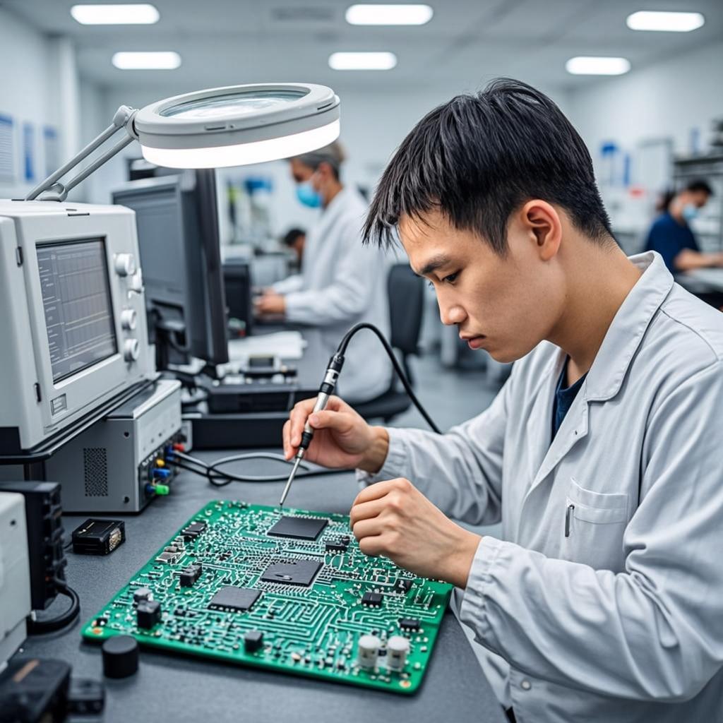
PCB assembly (PCBA) is the process of mounting electronic components on a PCB surface to make a fully operative electronic device. These parts, which are resistors, capacitors, and integrated circuits, as well as connectors, are picked and mounted onto the PCB in accordance with the design of the circuit. After it attach components, they are welded to the PCB using techniques like wave soldering, reflow soldering, or manual soldering in order to form electrical interconnections. After the assembly process of the circuit is done, it undergoes final inspection to check whether all the components of the electricity system have been placed correctly and soldered together properly. Further, these steps of functional and in-circuit test conduction are carried out in order to verify the functionality and performance. PCB assembly could also be tested for conformal coating or encapsulation, which will protect the assembly from environmental factors. PCBA plays a significant role in guaranteeing that electronic gadgets match up with quality specifications in their functioning as well as in producing devices that are durable and reliable for the intended application.
These are the types of PCB assemblies:
The Through-Hole Assembly (THA) is a technique in electronic circuit board mounting process in which the components’ leads or pins are inserted through the holes drilled into the board for the components to stand upright on the assembled board. Unlike SMT assembly, which transfers components directly onto the PCB board surface, THA goes through the underside of the board to solder component leads to their respective pads on the opposite side. The THA has been a traditional approach for multiple reasons, including the requirement of stronger connections or in the manufacture of low-volume assemblies. Parts were designed and manufactured with the THA due to its benefits over other assembly technologies Nevertheless, THA does retain significance where misplaced components that are meant for surface mounting are unsuitable, such as those that require more strength for mechanical purposes, and continuation with THA remains popular in aerospace and automotive companies due to their resilience and ease of inspection.
Nowadays, Surface Mount Technology (SMT) assembly is usually used for electronic circuit board assembly, whereas in through-hole assembly (THA), holes in the circuit board are previously drilled and components are soldered onto the circuit boards. In surface-mount technology, components are fastened to the board by the leads that would roll onto the top of the board, and then accessories are attached to pads that are the same size as the leads. Generally speaking, these assembly processes are operated by pick-and-place devices that move each component into the appropriate site determined by layout. SMT assembly has the following advantages over THA: high component density, smaller board size, and improved electrical performance due to the engineers of short signal path. It is currently one of the most broadly utilized techniques in modern industrial production of electronics for its productivity, competitive advantages, and adaption to miniaturization and large-scale manufacturing.
Mixed Technology Assembly combines Through-Hole Assembly (THA) and Surface Mount Technology (SMT) assembly onto the same printed circuit board (PCB), resulting from the increasing number of electronic devices that incorporate both types of assembly. The advantage of this technique is that it can use either surface mount or through-hole components in a single printed circuit board assembly, so that the strengths of the two types of technologies are combined. The most apparent advantage of through-hole components across the board is their solderable leads, which provide a robust mechanical connection liable to meet the needs of components with higher power handling or mechanical strength. Meanwhile, the surface mount components offer advantages in size, weight, and cost-effectiveness, among other measurable aspects. The mixed assembly technique is often applied in situations where a number of different components are used to cause a specific type of behavior or function or to achieve a given performance level, giving an option for different design and manufacturing.
The single-sided assembly, however, is an instance of a circuit board manufacturing process in which only one side of PCB is being populated with electronic components. The construction, which incorporates components by either through-hole components or innovative SMT assembly approaches, is mainly dependent on the specific project requirements. The single-sided board assembly technique is often employed in those uses where the size of the printed circuit boards is not an issue and the application space is not a major concern. It enables economies in production through single-side PCB manufacturing without the complexity of a double-sided or multiple copper layers. Meanwhile, though, it will reduce the packed density of part elements on the panel and will not be an ideal choice for more fixed electronic layouts.
Double-Sided Mounting, on the other hand, is a way of constructing electronic devices in which components are assembled on both front and reverse sides of the printed circuit board (PCB). Using this method, a more component-dense assembly and a greater fidelity of circuit designs can be achieved as compared to single-sided printed passive bare board assembly. In double-sided construction, parts could be mounted using both the through-hole assembly technique and the mount mount technique. The parts could then be placed according to preference and availability. This strategy is most commonly employed when place efficiency is important or if highly complex circuits are required where components are placed on both sides of the PCB. Double-sided assembly requires a lot more care and can also be challenging and time-consuming as compared to single-sided assembly due to the need for accurate and in-time component placement for soldering on both sides of the board. On the flip side, it opens new design possibilities and provides the platform to manufacture all the necessary electronic devices and applications as well.
The advanced Multi-Layer Assembly (MLA) method is a modern production technique that enables the creation of PCBs with more than two conduction layers separated by the insulating material. Through the extensions of linings, these layers can make contact through vias that will be useful for circuit designs with high component density and good signal quality. Multi-layer PCBs are a primary component in electronic devices that have little space for expansion and require high processing power, e.g., computers and smartphones. The completion of this assembly process is done using this method. It involves placement and precision alignment of layers, drilling of vias, plating with non-conductive substrate material, and lamination. The mounting of elements using these options, including whole assembly (THA) and mounting on the surface (SMT) technologies, offers a range of choices in design and functionalities. Despite seeming to be more complicated, the multi-layer process is basically an inherent property of modern electronic circuitry since it endows improved design flexibility, electrical performance, and reliability.
The PCB assembly process usually contains multiple steps, which start with the design of a circuit pattern and end with the examination and visual inspection (or testing) of the completed board. Here are the step-by-step process in PCB Assembly:
Design and Layout: Information engineers create PCB circuits that carry out special synthesis utilities considering signal routing, component placement, and thermal management, among others. They are responsible for ensuring the design of the product will comply with electrical and mechanical requirements, including EMC and signal integrity concerns.
Manufacturing the PCB: The very first step of the PCB assembly process is formatting the substrate material, which is usually FR-4-type epoxy laminate. The photolithography technique is utilized for the purpose of transferring the circuit layout onto the substrate, which is carried out by revealing the semiconductor via a process of being exposed to light through a mask, followed by chemical etching, which is used for the removal of unwanted copper traces.
Component Procurement: Purchasing specialists identify the components from the known suppliers and check for other goods that are of good quality and authentic. These items perform functions such as hindering components from deviating away from the limits set by the selection of bill of materials (BOM) in relation to tolerances, ratings, and package sizes.
Stenciling: A pre-formed stainless steel stencil made up to the overall PCB design pattern is placed over the board. Next, the board is screened from the front by means of applying solder paste, which is a mixture of solder mask particles and flux used to create an exact solder paste deposit on each pad area.
Component Placement: Robots do the same job as humans, with the PCB files guiding each robot to place components on the board at high speed. Such equipment can automatically position components accurately based on the vision system to the required tolerances.
Reflow Soldering: The reflow process in the oven then takes the PCB, which is now fully populated with components and solder paste. The precise temperature of the oven ensures the gradual heating of the board. While the soldering paste is melted, the solder joints between the components and PCB pads are formed and shaped into a solid state.
Through-Hole Component Insertion: Through holes are either drilled by hand or with automated insertion equipment to hold the components in the PCB. PCB leads are then cut to length, and the traces on the board will undergo soldering during the final PCB assembly process stage.
Cleaning: After successfully soldering the PCB, it goes through cleaning to get rid of flux residues and other contaminants. Generally, cleaning is done thoroughly so as to prevent contamination of any parts that may affect the PCB’s reliability and lifespan.
Inspection: The assembled PCB then goes through a rigorous quality control process involving checking from defects and errors through the various stages. Visual optical inspection (AOI) techniques and X-ray machines that facilitate the detection of faults like mispositioning, disparities or absence of components are used.
Testing and Quality Control: The manufactured PCB then goes through a tough battery of tests to attest to its functionality and general excellence. This can be accomplished by using electrical testing with the help of automated test equipment (ATE). It can also carry out boundary and short/open checks by a functional test to find out that the PCB operates the way it is expected.
Final Packaging: After performing tests and quality control checks, the PCB is finalized for engineering. Consequently, the PCB producers could apply protective coatings, stamp them with serial numbers or barcodes, and pack them anti-statically for shipments to the customers.
Documentation: Meticulous monitoring is undertaken at every point within the manufacturing system and all steps are recorded in order to maintain traceability. For the PCB record, relevant data traces are recorded, such as component sourcing records, assembly instructions, test results, and any changes made during the PCB process. This creates a chronological record of the manufacturing of the PCB.
Automated optical inspection (AOI) is a crucial element of PCBA; it provides the needed fault detection and electronic device reliability during the manufacturing process.
Here’s why Automatic Op