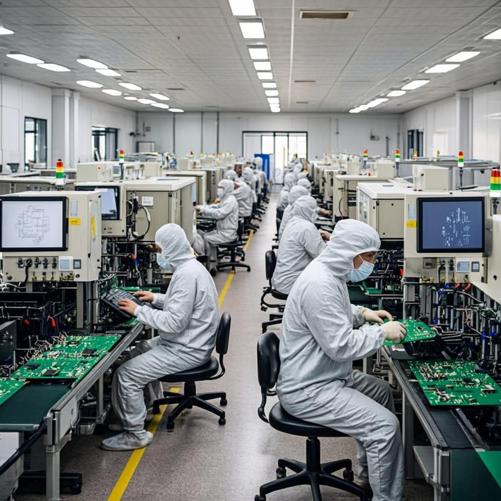
In the world of modern electronics, the Printed Circuit Board (PCB) serves as the foundational backbone, connecting disparate components into a cohesive, functional system. Among the various types, rigid PCBs remain paramount due to their durability, reliability, and widespread applicability across industries, from consumer gadgets to aerospace and medical devices.
This article delves into the evolving landscape of rigid PCB design, exploring advanced techniques that push the boundaries of performance and miniaturization, the critical role of seamless integration, and the sophisticated software tools that empower engineers to navigate these complexities and bring cutting-edge electronic innovations to life.
Modern rigid PCB technology achieves 99.9% dimensional stability through sophisticated substrate engineering and multi-layer lamination processes. A rigid printed circuit board represents a non-flexible electronic interconnection platform built upon a solid substrate material that provides mechanical support and electrical insulation for electronic components.
The fundamental physics underlying rigid PCB performance centers on the glass transition temperature (Tg) of the substrate material, typically 130-180°C for standard FR4, which determines thermal stability and operational reliability.
The mechanical properties of rigid PCBs derive from their composite structure, combining woven fiberglass reinforcement with epoxy resin matrices. Standard FR4 substrate exhibits tensile strength of 310 MPa and flexural strength of 415 MPa, providing exceptional durability for demanding applications.
The dielectric constant of FR4 ranges from 4.2-4.6 at 1 MHz, directly impacting signal propagation velocity according to the relationship: v = c / √(εr × μr) Where v represents signal velocity, c is the speed of light, εr is relative permittivity, and μr is relative permeability. This fundamental equation governs high-speed signal integrity calculations that are essential for modern digital systems operating above 100 MHz.
The rigid PCB architecture enables component density improvements of 300-500% compared to traditional wire-wrap techniques. It also ensures superior electromagnetic compatibility through controlled impedance design. Multilayer rigid PCBs can achieve up to 40 layers in advanced applications, with each additional layer increasing routing density by approximately 15-20%.
High-density interconnect (HDI) design methodologies revolutionize rigid PCB capability through microvias with diameters as small as 0.1mm and trace widths approaching 25 micrometers. The implementation of HDI technology in 2025 enables component density increases exceeding 400% while maintaining signal integrity through advanced electromagnetic field modeling.
Fig 1: HDI PCB featuring SMD components
Signal integrity analysis requires precise calculation of characteristic impedance using the following relationship for microstrip transmission lines: Z₀ = (87/√(εr+1.41)) × ln(5.98h/(0.8w+t)) Where h represents substrate height, w is trace width, t is copper thickness, and εr is dielectric constant. Modern rigid PCB designs target impedance tolerances within ±5% to ensure optimal signal transmission.
The design process for 2025 rigid PCB projects follows these critical steps:
Automated design rule checking (DRC) in modern CAD tools identifies 95% of potential manufacturing issues before fabrication, significantly reducing prototype iteration cycles. The integration of machine learning algorithms in PCB routing optimization demonstrates timing closure improvements of 40-60% for complex digital designs.
The automotive electronics sector represents the fastest-growing rigid PCB market segment, expanding at 8.2% CAGR through 2028. Electric vehicle applications demand rigid PCBs capable of operating across temperature ranges from -40°C to 125°C while maintaining functional reliability for 150,000+ thermal cycles. Tesla's Model S utilizes over 60 rigid PCBs throughout its electronic control systems, demonstrating the critical role of these components in modern automotive design.
Aerospace and defense applications leverage rigid PCBs operating in extreme environments with radiation tolerance up to 100 krad and vibration resistance meeting MIL-STD-810G standards. For instance, Boeing 787 aircraft incorporate over 2,000 rigid PCBs across avionics, flight control, and passenger entertainment systems. The aerospace sector requires thermal cycling from -55°C to 125°C for 2,000+ cycles without performance degradation.
5G infrastructure deployment drives demand for rigid PCBs supporting frequencies up to 28 GHz, requiring specialized low-loss dielectric materials with dissipation factors below 0.002. The telecommunications industry projects rigid PCB volume growth of 12% annually through 2027 as network densification accelerates.
Fig 2: Rigid PCB of a mobile phone
Medical device applications require rigid PCBs meeting IPC-6012DA Class 3 standards with enhanced reliability specifications. Pacemaker control circuits utilize rigid PCBs with MTBF ratings exceeding 20 years, achieved through component derating and hermetic packaging. The medical electronics market demands leakage currents below 10 microamperes to ensure patient safety, necessitating specialized substrate materials and manufacturing processes.
Rigid-flex PCB technology combines the mechanical stability of rigid boards with the dynamic flexibility of polyimide circuits, enabling 3D packaging solutions that reduce overall product volume by 40-60%. The manufacturing process utilizes no-flow prepregs costing $1.50-3.00 per square foot compared to $0.25 per square foot for standard prepregs, resulting in 7x higher costs than traditional rigid boards.
Bending radius calculations for flexible sections follow the relationship R ≥ 6t, where R represents the minimum bend radius and t is the total flexible stack thickness. Dynamic flexing applications require bend radii exceeding 10 times the flexible thickness to achieve 1 million+ flex cycles without failure. The integration of rigid and flexible sections demands precise impedance matching within ±10% across transition zones.
Common integration challenges include:
Fig 3 : A rigid PCB integrated with a flex PCB
Altium 2025 dominates the professional PCB design market with unified design environments supporting up to 40-layer stackups and integrated 3D mechanical collaboration. The latest version incorporates AI-powered component placement algorithms reducing design time by 35% while maintaining optimal thermal and electrical performance.
KiCad (Open Source Community, 2025) provides comprehensive PCB design capabilities with advanced 3D visualization and SPICE simulation integration at zero licensing cost. The platform supports multilayer designs up to 32 layers with professional-grade design rule checking and gerber export capabilities.
Advanced simulation capabilities in 2025 tools include electromagnetic field solving with convergence times under 30 minutes for complex 20+ layer designs. Thermal simulation accuracy improves to within ±3°C of measured values through enhanced material modeling and boundary condition handling.
Design for Manufacturing (DFM) checking algorithms identify 98% of potential fabrication issues during the design phase, including minimum trace width violations, via aspect ratio problems, and solder mask clearance errors. Automated optical inspection (AOI) integration provides real-time feedback with manufacturing partners, reducing prototype turnaround times from 10-14 days to 5-7 days.
Via aspect ratio limitations represent the most frequent rigid PCB failure mode, with ratios exceeding 12:1 causing plating reliability issues in standard manufacturing processes. HDI technology enables via aspect ratios up to 6:1 through laser drilling, providing superior reliability for high-density applications.
Critical design guidelines for 2025 rigid PCB implementations include: