Underfill is a critical PCBA encapsulation technique where a specialized epoxy resin or polymer adhesive is dispensed and cured to fill the microscopic gaps beneath semiconductor components (like flip chips, BGAs, or CSPs) and the PCB substrate.
Underfill technology is a critical PCBA protection method that safeguards semiconductor devices (such as flip chips, BGAs, and CSPs) from mechanical stress, including shock, drop, and vibration. Additionally, it minimizes solder joint strain caused by CTE (Coefficient of Thermal Expansion) mismatch between the silicon die (chip) and the PCB substrate—two materials with different thermal expansion rates.
The underfill material—a specialized liquid polymer adhesive—is dispensed onto the populated PCB after reflow soldering. Once applied, the underfill epoxy flows via capillary action, filling the microscopic gaps beneath the semiconductor component. After dispensing, the underfill undergoes thermal or UV curing, forming a rigid encapsulation layer that reinforces the interconnect solder joints between the chip’s underside and the PCB’s surface.
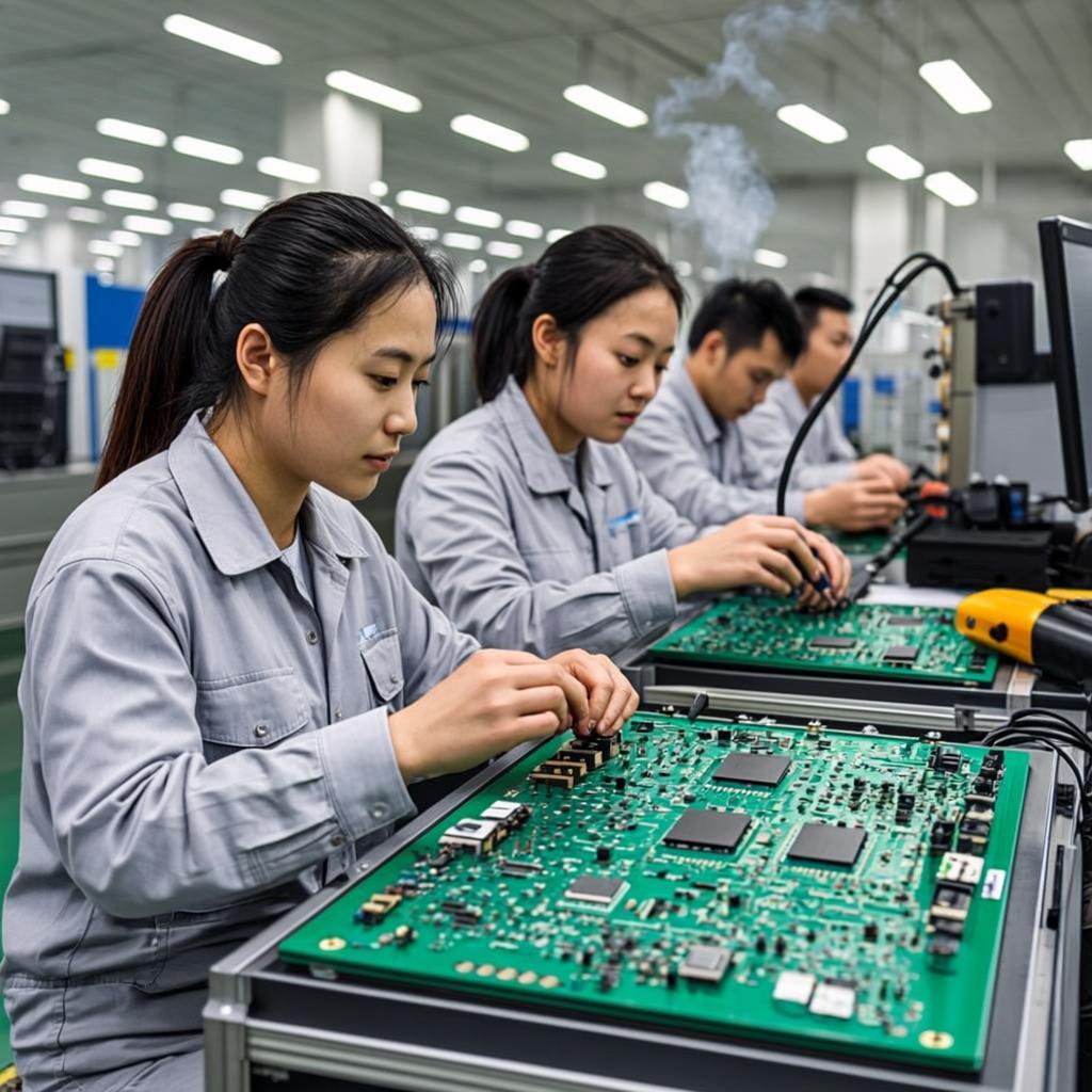
Successful underfill encapsulation demands rigorous process expertise. Precise control of epoxy temperature, resin-to-hardener ratios, and dispensing parameters is critical to achieve consistent, void-free underfill results. Proper material mixing and controlled application ensure optimal flow characteristics and reliable solder joint protection beneath components.
WELLER develops specialized underfill techniques for targeted protection. For assemblies requiring selective encapsulation (not full-board coverage), we engineer custom solutions like fence-and-fill tooling. This precision approach maintains high-reliability standards while optimizing manufacturing costs.
As your innovation partner, WELLER continuously advances our electronic manufacturing processes. We pioneer cutting-edge underfill technologies and potting methodologies to deliver globally supported, reliability-focused solutions for mission-critical PCBAs.