Published Date May 9, 2022 Author Cadence PCB Solutions
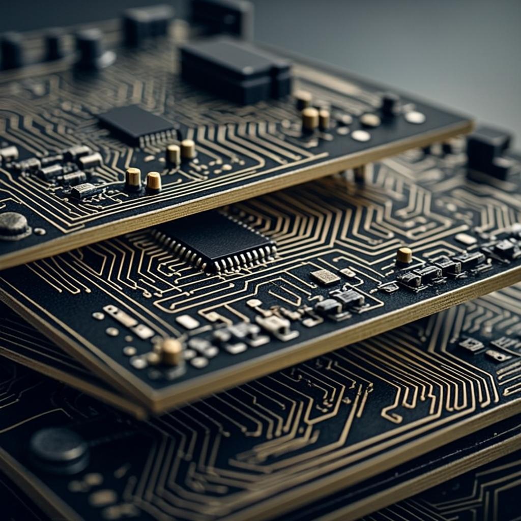
Many experts consider ceramic PCBs more advantageous than traditional FR4 PCBs. Even though ceramic PCBs are relatively new on the PCB substrate list, they are gaining popularity for use in high-density electronic circuits. Why? The versatility, durability, stability, and insulation properties offered by ceramic PCBs make them more advantageous than traditional PCBs. And, ceramic PCBs support circuit miniaturization without compromising precision and reliability. In this article, we will discuss the types of ceramic PCBs and learn what makes them so advantageous.
For PCBs placed in environments of high pressure or high temperature, traditional PCB substrate materials may exhibit flaws in extreme conditions. However, ceramic PCB substrate material is suitable for high temperature and pressure as well as corrosive or vibrational circuit conditions. Ceramic PCBs have a high thermal conductivity as well as coefficient of thermal expansion. These PCBs are most suitable for high power density circuit designs that are used in extreme conditions, especially in the aerospace and automotive industries.
Ceramic PCBs are made from a range of ceramic materials. The thermal conductivity and coefficient of thermal expansion (CTE) are the main two properties to focus on when selecting ceramic materials. The ceramic materials used in PCBs refer to a class of substrate materials such as aluminum nitride (AlN), alumina (Al2O3), beryllium oxide (BeO), silicon carbide (SiC), and boron nitride (BN). These ceramic materials share similar chemical and physical properties. Below, we will explore the properties of three common ceramic materials.
The three most commonly used ceramic materials for PCB manufacturing are:
Alumina (Al2O3) - The mechanical strength, chemical stability, thermal conductivity, and electrical properties of Al2O3 are advantageous compared to other oxide ceramics. The abundance of raw material makes alumina the most commonly used ceramic substrate material. Al2O3 ceramic PCBs are used in automobile sensor circuits, shock absorbers, and engines. The high thermal stability of Al2O3 ceramic PCBs improves the performance and thermal efficiency of the circuits used in automobiles.
Aluminum Nitride (AlN) - The high thermal conductivity and coefficient of expansion are two properties that make AlN noteworthy as a substrate material in the PCB industry. The thermal conductivity of AlN varies in the range of 170 W/mK to 220W/mK. The CTE of AlN ceramic matches with silicon semiconductor chips, which establishes a good bonding between the two, thus making their assembly reliable. AIN is used in sensor circuits in automobiles, as it can withstand extreme temperatures, corrosion, and vibration while providing efficient, accurate, and sensitive sensor signals.
Beryllium Oxide (BeO) - BeO is a ceramic PCB substrate material with a thermal conductivity around nine times that of Al2O3 and greater than metal aluminum. BeO showcases better chemical stability than AlN and high electrical isolation comparable with Al2O3e. BeO is used in applications where the PCB is subjected to high temperatures or in high-density PCBs facing space limitations to provide air or liquid cooling.
The manufacturing process of ceramic PCBs is simpler than traditional PCBs. Thermally conductive ceramic powder and an organic adhesive are mixed together and thermally treated to fabricate ceramic PCBs. Usually, laser rapid activation metallization (LAM) technology is utilized for ceramic PCB manufacturing. Apart from the ceramic material used, there is one more classification in ceramic PCBs based on the manufacturing process:
Ceramic PCBs are well suited for high-temperature, high pressure, high frequency, and high insulation performance. The extensive design, simulation, and analysis features available from Cadence can assist designers in designing PCBs from any material, including ceramics.
Leading electronics providers rely on Cadence products to optimize power, space, and energy needs for a wide variety of market applications. If you’re looking to learn more about our innovative solutions, talk to our team of experts or subscribe to our YouTube channel.
Cadence PCB Solutions is a passionate writer and expert in the field of PCB design and electronic engineering. With years of experience in developing innovative solutions for complex circuit designs, Cadence PCB Solutions specializes in breaking down technical concepts into clear, actionable insights for engineers, hobbyists, and industry professionals alike.
Evaluate how our PCB software fits in your design workflow.