Multi Layer Printed Circuit Board Assembly (ML PCBs) have emerged as a cornerstone solution, enabling the integration of complex circuitry into a smaller footprint. This article delves into the intricacies of multilayer PCB assembly, exploring its applications, benefits, challenges, and best practices.
In today’s technologically advanced world, the demand for compact, high-performance electronic devices has skyrocketed.
Q: What is the difference between a multilayer PCB and a flexible PCB? A: A multilayer PCB has multiple layers of circuitry stacked on top of each other, while a flexible PCB is made from a flexible substrate that allows for bending and folding.
Q: How many layers can a multilayer printed circuit board assembly have? A:The number of layers in a multilayer PCB can vary widely, ranging from a few to several dozen.
Q: What are the common materials used for multilayer printed circuit board assembly?
A: Common materials include FR-4 (epoxy glass), high-temperature FR-4, polyimide, and Teflon.
Q: What are the key factors to consider when selecting a multilayer PCB manufacturer? A: Key factors include manufacturing capabilities, quality control measures, lead times, and pricing.
Q: What are the future trends in multilayer printed circuit board assembly technology? A: Future trends include the development of even denser PCBs, the use of advanced materials, and the integration of embedded components.
Q: What are the common design software tools used for multilayer printed circuit board assembly?
A:Popular tools include Altium Designer, Autodesk Eagle, and KiCad.
Q: How do I ensure signal integrity in multilayer printed circuit board assembly?
A:Use impedance-controlled routing, minimize vias, and carefully consider trace lengths and widths.
Q: What factors influence the cost of multilayer printed circuit board assembly?
A: Factors include the number of layers, component density, board size, and manufacturing complexity.
Q: How can I reduce the risk of manufacturing defects in multilayer printed circuit board assembly?
A: Implement robust quality control measures, use high-quality materials, and adhere to industry standards.
Q: What are the emerging applications of multilayer printed circuit board assembly in the automotive industry?
A: Advanced driver assistance systems (ADAS), electric vehicles (EVs), and autonomous vehicles are driving the demand for complex multilayer PCBs.
Q: How are multilayer printed circuit board assembly used in wearable technology?
A: Wearable devices often incorporate multilayer PCBs to integrate sensors, processors, and wireless communication modules into a compact form factor.
Q: What are the future trends in multilayer PCB technology?A: Trends include the development of flexible PCBs, embedded components, and advanced materials with improved thermal and electrical properties.
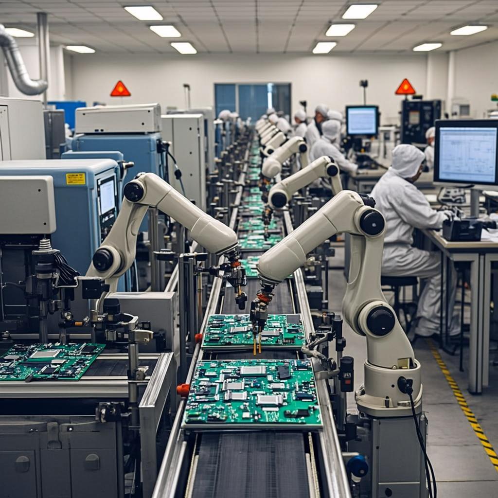
Printed circuit board assembly (PCBA)is a crucial process in the manufacturing of electronic devices. It involves the attachment of various electronic components, such as resistors, capacitors, and integrated circuits, onto a printed circuit board (PCB). The PCB serves as a foundation for interconnecting these components, creating functional electrical circuits.
The PCBA process typically involves several key steps:
PCBA is a critical process in a wide range of industries, including electronics, automotive, medical, and audio. It enables the creation of complex electronic devices with miniaturized designs and enhanced performance.
Advancements in PCBA technology, such as automated assembly lines and advanced inspection techniques, have contributed to the increased efficiency and reliability of the process.
Q: How can I make my multilayer printed circuit board assembly more environmentally friendly?
A: Choose materials with lower environmental impact, reduce waste during manufacturing, and implement energy-efficient processes.
Q: What are the challenges associated with recycling multilayer printed circuit board assembly?
A:The presence of hazardous materials and the complexity of the manufacturing process can make recycling difficult.
Q: How can I ensure responsible sourcing of materials for my multilayer printed circuit board assembly?
A: Work with suppliers who adhere to ethical and sustainable practices.
Multi Layer Printed Circuit Board Assembly, as the name suggests, are boards with multiple layers of copper circuitry separated by insulating materials. The layers are interconnected through vias, enabling intricate circuitry and precise component placement. Multilayer PCBs offer distinct advantages over single-layer or double-layer PCBs.
MultilayerPrinted Circuit Board Assembly are widely used across various industries due to their versatility and performance benefits. Some common applications include:
Multilayer printed circuit board assembly involves several critical steps:
While multilayer printed circuit board assembly offer numerous advantages, their assembly presents unique challenges:
Design for Manufacturability (DFM): Incorporate DFM principles throughout the design process to minimize manufacturing challenges and improve yields.
Multilayer PCBs have become an indispensable component in modern electronic devices. Their ability to integrate complex circuitry into a compact form factor has revolutionized various industries.
By understanding the benefits, challenges, and best practices associated with multilayer PCB assembly, engineers and manufacturers can leverage this technology to create innovative and high-performance products.
By incorporating these additional takeaways into your multilayer PCB assembly process, you can enhance product reliability, reduce costs, and stay competitive in today’s demanding market.