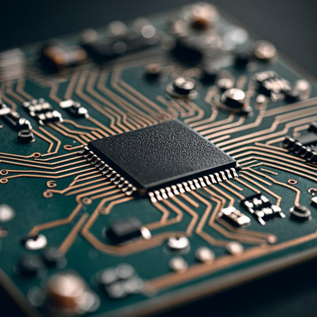
Printed Circuit Board Assembly (PCBA) manufacturing is the process of attaching electronic components onto a printed circuit board (PCB) to create a fully functional electronic assembly. Unlike a bare PCB, which is simply the board with etched circuits, PCBA combines the board with all required components—resistors, capacitors, integrated circuits, connectors, and more—through precise soldering and assembly processes.
The key difference between PCB and PCBA lies in functionality: a PCB alone is passive and cannot perform any electronic operation. Once components are assembled, it becomes a PCBA capable of powering devices, processing signals, or communicating with other systems. For example, a bare PCB might contain the printed copper traces for a smartphone motherboard, but only after assembly with chips, connectors, and other components does it become the working motherboard.
PCBA manufacturing is critical in modern electronics because it enables the miniaturization, reliability, and high performance required in today’s devices. From smartphones to wearable devices and industrial control systems, almost every electronic product depends on precise and high-quality PCBA to function correctly. Without proper assembly processes, even the most sophisticated PCB designs cannot achieve the desired performance or longevity.
Reliability and performance improvements are among the most significant advantages of well-executed PCBA manufacturing. High-quality assembly ensures that all components are properly placed, soldered, and electrically connected, reducing the risk of failures caused by poor connections, short circuits, or component misalignment. For instance, automotive electronics require strict reliability because a single failure could compromise safety.
Cost efficiency and scalability are additional benefits. Accurate assembly reduces waste from defective boards and minimizes rework costs. Standardized processes allow manufacturers to scale production efficiently while maintaining quality. For example, IoT device producers can mass-produce boards with consistent quality across hundreds of thousands of units, keeping production costs under control.
Real-world examples highlight the impact of high-quality PCBA. Smartphones rely on densely packed boards with multiple layers and tiny components; even a small assembly error can affect signal integrity or battery life. Industrial IoT devices need robust PCBA capable of withstanding harsh environments while maintaining connectivity and performance. In both cases, proper PCBA manufacturing ensures the final product meets reliability, durability, and functional expectations.
PCB fabrication is the process of creating the bare circuit board before components are added. Key steps include:
Transitioning to PCB assembly involves taking the fabricated board and attaching all electronic components to form a fully functional PCBA. The assembly process includes solder paste application, component placement, soldering, and inspection.
Comparison:
SMT is the most widely used PCBA process for modern electronics. It involves mounting components directly onto the surface of the PCB.
Step-by-step SMT process:
Common components used in SMT:
Example: High-volume smartphone PCBA uses SMT for millions of tiny components, allowing fast production with high precision and minimal human intervention.
THT involves inserting component leads through pre-drilled holes in the PCB and soldering them on the opposite side.
Step-by-step THT process:
Comparison with SMT:
Example: Industrial machinery PCBA often uses THT for power connectors and heavy-duty components to ensure long-term reliability.
Mixed technology combines SMT and THT on the same board to leverage the advantages of both.
Best practices for hybrid assemblies:
This approach is common in high-performance or industrial boards that need both fine-pitch ICs and strong mechanical connectors.
Quality control ensures that PCBAs are reliable and defect-free.
In-process inspection:
Final inspection:
Step-by-step defect detection workflow:
This structured approach ensures that every PCBA meets performance, reliability, and safety standards.
The PCB substrate is the foundational material that supports circuits and components. Common types include:
Selection criteria for PCB substrates include:
Example: A high-speed communication board may use Rogers or a low-Dk material to reduce signal loss, whereas a standard consumer device can use FR4 to balance cost and performance.
PCBA relies on both passive and active components:
Sourcing considerations for reliability:
Example: Automotive PCBA may require capacitors rated for wide temperature ranges and ICs with automotive-grade certifications to ensure long-term reliability.
Solder and flux are essential for creating strong electrical and mechanical connections.
Leaded vs. lead-free solder:
Flux types and their roles:
Example: For high-temperature PCBA applications, such as industrial motor controllers, SAC305 lead-free solder with rosin-based flux may be chosen to ensure strong connections without component damage during reflow.
Design for Manufacturability (DFM) focuses on creating PCB designs that are easy and cost-effective to manufacture while minimizing assembly errors. Key guidelines include:
Example: On a high-density board, increasing trace width from 4 mils to 6 mils for power traces can improve yield and reduce solder defects without significantly increasing board size.
Design for Testability (DFT) ensures that boards can be easily tested and troubleshooted during production and maintenance.
Key strategies:
Step-by-step approach to ensure testability:
Example: An industrial IoT board might include dedicated voltage test points for each power rail to quickly identify faults during assembly or field maintenance.
High-frequency or high-speed boards require careful design to maintain signal integrity, avoiding signal loss, reflections, and crosstalk.
Importance: Poor signal integrity can lead to communication errors, data loss, or device malfunction in applications like 5G, high-speed data converters, or advanced processors.
Techniques for reliable high-speed PCBA design:
Comparison of good vs. poor layout impact:
Example: On a high-speed networking board, using proper differential pair routing and controlled impedance can reduce bit error rates from 10^-9 to below 10^-12, improving overall reliability.
Optimizing PCBA manufacturing processes improves efficiency, reduces errors, and lowers production costs.
Lean manufacturing principles are widely applied: