Alumina (Al2O3) and Aluminum Nitride (AlN) ceramic PCBs with DBC/DPC copper, high thermal conductivity up to 170–190 W/m·K (one hundred seventy to one hundred ninety watts per meter-kelvin), and stable RF performance. Ideal for power modules, RF front-ends and LED engines operating from −55°C to +250°C (minus fifty-five to plus two hundred fifty degrees Celsius).
Thermal path efficiency and RF stability in harsh environments
Ceramic substrates provide a direct thermal path from junction to heat sink, enabling reliable operation under high power density and temperature cycling. DBC bonds thick copper to ceramic for low thermal resistance; DPC supports thin-film precision for RF microstrip and coplanar lines. Compared with FR-4, ceramics maintain dielectric stability up to 10–20 GHz (ten to twenty gigahertz) with minimal drift in Dk/Df.
Critical Risk: CTE mismatch between die, substrate and package can accelerate solder fatigue and delamination under −55↔+250°C (minus fifty-five to plus two hundred fifty degrees Celsius) cycling.
Our Solution: AlN (CTE ~4.5 ppm/°C — approximately four point five parts per million per degree Celsius) closely matches silicon, while Alumina provides a cost-effective baseline. We model stress with FEA, validate solder integrity via thermal shock and add design-for-reliability gates such as void limits and bond pull tests.
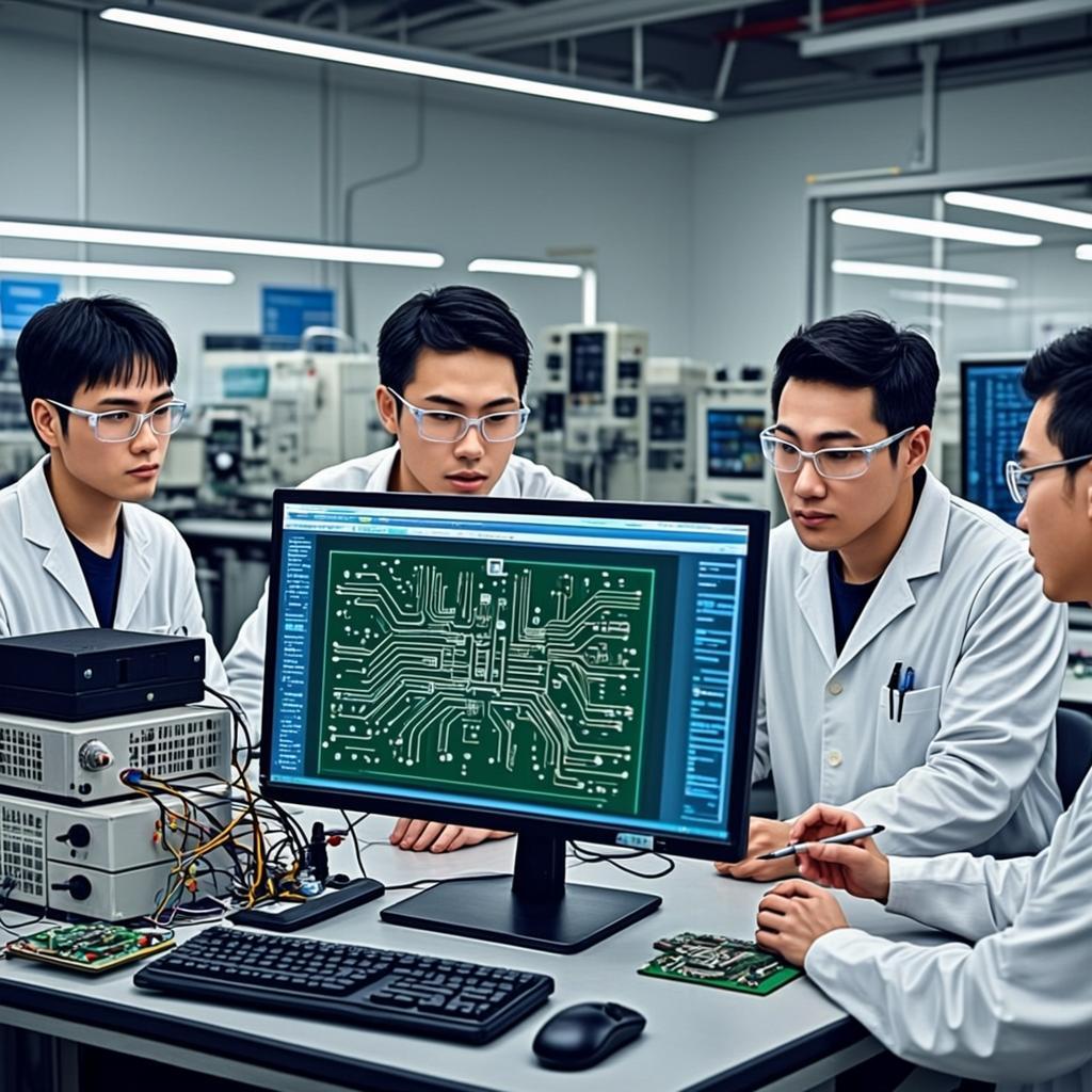
Process control and material traceability for critical applications
DBC uses high-temperature bonding to attach copper foils to ceramic with bond strength validated by peel tests exceeding 1.4 N/mm (one point four newtons per millimeter). DPC deposits metal via thin-film processes for fine-line control, supporting 50/50 µm (fifty/fifty micrometers) trace/space. LTCC cofiring integrates multilayer ceramics with embedded conductors and vias for compact RF modules.
Key parameters are monitored with SPC: copper thickness variation within ±10% (plus/minus ten percent), metal adhesion, and via quality. RF performance is verified with TDR and VNA to ensure impedance within ±5% (plus/minus five percent) for microstrip/differential pairs.
DBC/DPC/LTCC flows with reliability screening and full traceability
Choose AlN when heat flux and CTE matching dominate; choose Alumina for cost-sensitive RF or LED platforms where thermal density is moderate. For extreme heat density or when FR-4 hybridization is required, consider layering with low-loss materials. When using BeO (Beryllium Oxide) in legacy designs, we handle it under strict safety and compliance controls throughout manufacturing and waste management.
RF structures are verified with VNA for S-parameters and with TDR for impedance within ±5% (plus/minus five percent). We use on-board coupons or independent coupons depending on panel density and routing proximity. Power modules undergo thermal shock and burn-in to precipitate early-life failures before field deployment.
Ceramic PCBs are used in automotive power modules, RF front-ends, laser drivers and high-brightness LED engines.
Experience: Each ceramic PCB program undergoes comprehensive thermal modeling and power cycling validation to ensure long-term reliability under extreme environments. Finite element analysis (FEA) is applied to evaluate CTE mismatch between substrates, metallization and components, preventing solder fatigue from −55°C to +350°C (minus fifty-five to plus three hundred fifty degrees Celsius).
Expertise: We optimize DBC and DPC parameters — copper thickness, adhesion layer diffusion and oxide management — to maintain void-free bonding and flatness within ±20 µm (plus/minus twenty micrometers). Dielectric and insulation resistance are verified through 100% automated testing.
Authoritativeness: Builds comply with IPC-6012DS, MIL-PRF-31032 and ISO 9001, with audit readiness under IATF 16949 and ISO 13485. Certificates of conformance and test summaries are linked in MES for full traceability.
Trustworthiness: Lots are serialized and cross-referenced with thermal cycle and solderability reports; data integrity is maintained under calibrated equipment and digital traveler systems.
AlN matches silicon CTE (~4.5 ppm/°C — approximately four point five parts per million per degree Celsius) and offers 170–190 W/m·K (one hundred seventy to one hundred ninety watts per meter-kelvin) thermal conductivity for high-power designs. Alumina is cost-effective for moderate heat and RF. We can run FEA to validate stress, solder joints and vias before pilot builds.
BOM, stackup intent, Gerber/ODB++, RF specs if applicable, test plan, target operating temperature, expected heat flux and whether you need wire-bondable finishes. If die attach or chip-on-board is required, please include bonding method and any hermetic sealing constraints.
We use VNA for S-parameters and TDR for impedance correlation within ±5% (plus/minus five percent). Depending on density, we use on-board or independent coupons. For power modules and RF front-ends, we also run burn-in or thermal shock to screen early-life failures.
Yes. Options include ENEPIG, soft/hard gold, wire-bondable finishes, selective thick copper and hermetic sealing provisions. Traceability links material lots and coupons to serialized units for auditability.
From simple prototypes to complex production runs, our world-class factory delivers superior quality, fast turnaround and competitive pricing. Join thousands of satisfied customers who trust us with their PCB manufacturing needs.