The electronic devices that we use almost every day and everywhere consist of printed circuit boards (PCBs) that contain the components acting together to accomplish different functionalities. The design and manufacturing of these PCBs must go through processes to ensure a defect-free product that consumers can conveniently use. This requires the PCB to go through the last step, that is, testing.
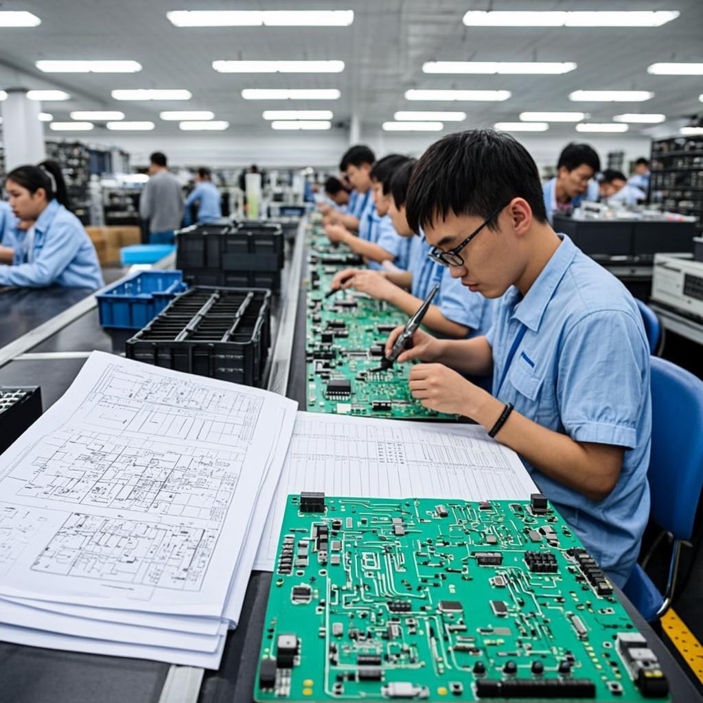
Printed Circuit Board Assembly, also called ‘PCBA’ for short, involves a series of processing steps to mount or place the electronic components on the printed circuit boards. PCBA starts by stencil printing a solder paste into the boards, and then placing the parts of different types, functions, and sizes on the pre-printed paste. The next step is to subject the boards with components to reflow to completely cure the paste and achieve a reliable joint. The assembled boards are then inspected using a high-speed machine with a vision system which is automatically operated.
PCBA does not end after optical inspection. A PCB can be visually good but electrically defective. This is where the PCBA Testing comes into play. PCBA Testing is the process of electrically testing the assembled boards to screen for any manufacturing flaws, material defects or board design issues.
The first type of PCB assembly testing that is most used for large-volume PCBA production is In-Circuit Testing(ICT). In-circuit testing is a bed-of-nails type of PCB assembly testing that can perform simultaneous testing of the PCB contact points through a customized fixture. Both the diagnostic and testing times are relatively faster for in-circuit circuit card assembly testing. The weakness of ICT is that it has less flexibility since it can only cater to a single type of PCB and is high-priced due to its complex software program and costly tooling. An in-circuit tester can be stand-alone or integrated with a functional test system for more efficient fault coverage and throughput.
The more flexible type of testing is called Flying Probe Testing which uses a probe that can move or fly to test the PCB. It can test fine-pitched devices but is relatively slower than ICT making it a more suitable technique for prototyping and small-scale production. It has a short development time and can easily be revised according to PCB layout changes unlike with ICT wherein expensive revision of the testers will be required.
The third type of circuit card assembly testing is called Functional Testing. This circuit card assembly testing method takes a longer time since the boards are being tested for all their functionalities, ensuring that the boards will work according to requirements using introducing stimuli and measuring the response of the boards. Functional circuit card assembly testing also has expensive design and development.
Take note, however, that 100% test coverage of all components is not possible due to considerable factors like stray impedance, cost, and processing time. To increase confidence in test coverage, PCBA companies would sometimes implement both ICT and functional testing.
Other in-process and offline controls during assembly must also be implemented such as stencil print inspection, automated optical inspection (AOI) and X-ray inspection to further strengthen the quality of the PCBs. Below are details explaining each inspection process:
After stencil printing the solder paste on the PCBs, the position, volume, and formation of the paste are inspected by a stencil printing inspection machine. The volume of the solder paste is measured relative to the aperture volume. The alignment of the solder paste is also checked during this inspection process which is typically measured in terms of width and length.
Automated Optical Inspection (AOI) is a rapid inspection technique that can check for missing components, misalignment, tombstoning, and other visual defects that break the supposed image of the PCB. Using a vision system software, a camera scans an