In the world of electronics, printed circuit boards (PCBs) are the backbone of functionality. But what if they could be more than just technical components? With 8-layer PCB art, you can create designs that are both functional and visually stunning. Let's dive into the exciting realm of PCB art design, exploring creative PCB layouts, artistic PCB projects, and how to use a PCB as a canvas while maintaining its core functionality. Whether you're an engineer, designer, or hobbyist, you'll find practical tips and inspiration to elevate your next project with functional PCB art.
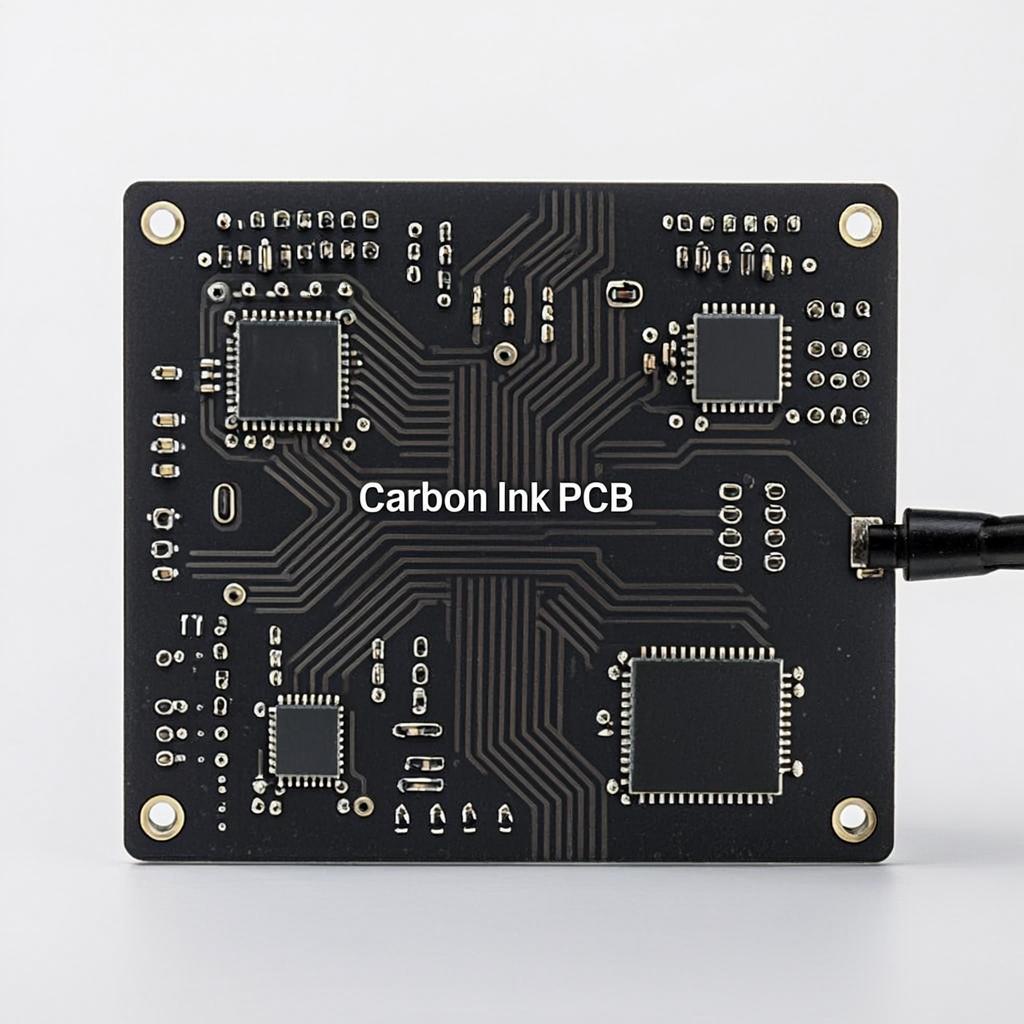
At its core, 8-layer PCB art is the fusion of technical design and aesthetic creativity on a multi-layered circuit board. An 8 layer PCB consists of eight conductive layers separated by insulating materials, often used in complex electronics like high-speed communication devices or advanced computing systems. By leveraging these layers, designers can craft intricate patterns, images, or textures on the board's surface or within its internal layers, turning a functional piece into a work of art.
Unlike the single or double layer PCB, an 8-layer PCB offers more space for creative PCB layouts. You can dedicate specific layers to artistic elements while reserving others for critical electrical routing. This balance ensures that the board remains fully functional while showcasing stunning visual designs. Think of it as turning a PCB into a canvas where every trace, via, and silkscreen contributes to both form and function.
Creating artistic PCB projects with an 8-layer board offers unique advantages over simpler designs. Here’s why this approach stands out for functional PCB art:
These benefits make 8-layer PCBs a perfect choice for designers looking to push the boundaries of creativity without sacrificing functionality.
Designing an 8-layer PCB that balances art and function requires careful planning. Below are actionable steps to guide you through the process of creating creative PCB layouts and artistic PCB projects.
Start by deciding what kind of visual impact you want your PCB to have. Are you aiming for a minimalist pattern, a detailed image, or a thematic design like a circuit board inspired by nature? Keep in mind that your PCB art design should complement its purpose. For example, if the board is for a gaming device, you might incorporate pixelated graphics or joystick silhouettes into the silkscreen layer.
Remember to consider how the artistic elements will fit within the constraints of an 8-layer structure. Plan which layers will hold the artwork and which will focus on electrical routing to avoid signal interference.
To bring your vision to life, you'll need design software that supports multi-layer PCB layouts and allows for creative freedom. Many popular tools offer features to import images or draw custom shapes directly onto the board. Look for software with robust layer management to assign specific layers for art while keeping others dedicated to functionality.
For artistic elements, focus on the silkscreen layer (used for text and symbols) and copper layers for conductive patterns that double as art. Ensure the software supports high-resolution imports if you're converting an image into a PCB trace or silkscreen design.
In an 8-layer PCB, each layer serves a purpose. Here’s a typical breakdown to balance creative PCB layouts with functionality:
By separating art from critical components, you ensure the board remains functional while showcasing your artistic PCB project.
One of the biggest challenges in functional PCB art is ensuring that artistic additions don’t interfere with electrical performance. Here are some tips to maintain balance:
The materials and finishes you choose for your 8-layer PCB can enhance its artistic appeal. Consider the following options:
These choices not only improve aesthetics but also protect the board, ensuring it remains functional in real-world applications.
Before finalizing your design, create a prototype to test both the functionality and visual impact of your artistic PCB project. Check for issues like signal integrity (ensuring minimal crosstalk at high frequencies, such as 5 GHz for wireless applications) and verify that the artwork aligns with your vision. Use feedback from testing to refine the design, adjusting artistic elements or routing as needed.
Need ideas for your next 8-layer PCB art project? Here are a few creative concepts to spark inspiration:
While designing functional PCB art on an 8-layer board is rewarding, it comes with challenges. Here’s how to address common issues:
Functional PCB art isn’t just for show—it has real-world applications across various industries. Here are a few examples:
If you’re new to creating artistic PCB projects, start with these beginner-friendly tips:
8-layer PCB art opens up a world of possibilities for designers and engineers who want to combine creativity with cutting-edge technology. By treating a PCB as a canvas, you can craft creative PCB layouts and artistic PCB projects that are both functional and beautiful. From planning your design across multiple layers to choosing the right materials for visual impact, every step offers a chance to innovate. With careful attention to detail and a balance of art and engineering, your 8-layer PCB can become a masterpiece that stands out in both performance and aesthetics.
Whether you’re working on a personal project or a professional product, functional PCB art allows you to push boundaries and make a lasting impression. Dive into the world of PCB art design today and transform your circuit boards into something extraordinary.