Helen Frankenthaler PCB Circuit Board R&D Center

Ceramic HDI PCB for Smart Home

HDI PCB | Best Custom PCB Assembly Service

HDI PCB

HDI PCB technology creates many possibilities in a wide range of industries. To save manufacturing time and improve productivity, HDI technology is a very good choice.

HDI pcb introduction

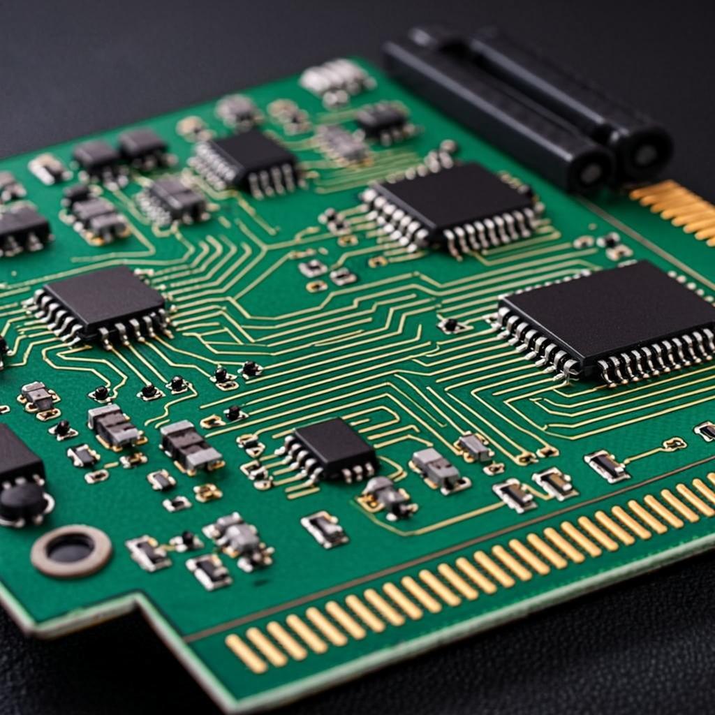
High-density interconnection (HDI) PCB represents one of the fastest development technologies in PCBA processing. Because its circuit density is higher than that of traditional PCBA circuit boards, the HDI PCB design can contain smaller pores and capture pads, as well as higher -connected pad density. The HDI board contains blind holes and buried holes, and usually contains micro holes with a diameter of 0.006 or smaller.

By using HDI technology, designers can now place more components on both sides of the original PCB. With the development of pores and blind hole technology in pads, it allows designers to place smaller components together. This means faster signal transmission and significantly reduce signal loss and cross -delay.

The advantage of HDI PCB

The development of PCB HDI technology provides engineers with greater design freedom and flexibility than ever. If necessary, designers using HDI high-density interconnection methods can now place more components on both sides of the original PCB. In essence, HDI PCB provides designers with more working space, and at the same time allows them to place smaller components closer. This means that high-density interconnection PCB will eventually bring faster signal transmission and higher signal quality.

  • The wiring is more dense
  • The power is more stable
  • Reduce EMC interference
  • Improve signal integrity
  • Accelerate the development of multi-layer PCB
  • Suitable for SMD paste
  • More component space

Give me a message

If you have a PCB project, please leave me a message, we will give you a free offer within 24 hours.

HDI PCB Applications

HDI boards are appropriate for a wide range of industries. As mentioned above, you’ll find them in all types of digital devices, like smartphones and tablets, where miniaturization is key to the effective application of the product. You can also find high-density interconnect PCBs in automobiles, aircraft and other vehicles that rely on electronics.

One of the most critical areas where the high-density PCB is making huge inroads is in the medical arena. Medical devices frequently need small packages with high transmission rates that only HDI PCBs can supply. For example, an implant needs to be small enough to fit in the human body, but any electronics involved in that implant absolutely must efficiently allow for high-speed signal transmission. Here, the HDI PCB indeed is a godsend. HDI PCBs can also be useful in other medical equipment, like emergency room monitors, CT scans and much more.

No matter your industry, you’re probably already getting some ideas about how high-density interconnect PCBs can make the electronics you produce or use even better-get in touch with us LSTpcb to discuss it. We’ll let you know if you’re on the right track and help you decide exactly how beneficial an HDI PCB can be to your industry. Then, you can determine whether or not to take the next step.

Our ability

project unitParameter/model
HDI Structure1+N+1、2+N+2、3+N+3、4+N+4、5+N+5、6+N+6、anylayer
Structure orderN+N、N+X+N、1+(N+X+N)+1
Number of layers that can be created1-42 layers
Minimum line width/spacing Unit: mil2\2
Minimum mechanical holes Unit: mm0.15mm
Minimum core plate thickness Unit: mil2mil
Laser hole diameter Unit: mm0.075mm-0.1mm
Minimum thickness of insulation layer Unit: mil2mil
Maximum diameter of resin plug hole Unit: mm0.4mm
Plated hole diameter Unit: mil3-5mil
Distance from the wall to the line of the smallest hole Unit: mil7mil
Laser hole accuracy Unit: mm0.025mm
Minimum BGA pad center distance Unit: mm0.3mm
Minimum SMT Unit: mm0.25mm
Plated Hole Depression Unit: um≤10um
Back Drill/Controlled Deep Drill Tolerance Unit: mm±0.05mm
Through-hole plating through-hole capability Proportion16:01
Blind Hole Plating Through Hole Capability Proportion1.2:1
Minimum BGA Pad Unit: mm0.2
Minimum hole diameter (mechanical drilling)Unit: mm0.2
Minimum buried hole diameter (laser drilling)Unit: mm0.1
Minimum Blind Hole Diameter (Laser Drilled)Unit: mm0.1
Minimum Blind Hole Diameter (Mechanical Drilling)Unit: mm0.2
Minimum spacing between laser blind holes and mechanically drilled holes Unit: mm0.2
Minimum Laser Drilled Hole Diameter Unit: mm0.10(depths≤55um)、0.13(depths≤100um)
Minimum BGA pad center distance Unit: mm0.3
Interlayer Alignment Unit: mm±0.05mm(±0.002″)

Related Products

AMB Ceramic Copper-Clad Substrate
  • Layers: 2 layers
  • Board Thickness: 0.635mm ± 0.05mm
  • Substrate Material: 96% Silicon Nitride
  • Surface Finish: ENIG (Electroless Nickel Immersion Gold)
  • Thermal Conductivity of Insulating Layer: 85 W/m·K
  • Outer Copper Thickness: 200μm
  • Gold Thickness: ≥ 3μ”
  • Process Characteristics: AMB process
DPC Aluminum Oxide Double-Sided ENIG/Silver Ceramic Substrate
  • Layers: 2 layers
  • Board Thickness: 0.5 mm
  • Base Material: Aluminum Oxide
  • Copper Thickness: 100 μm
  • Process Feature: DPC (Direct Plated Copper) Process
  • Surface Finish: ENIG / Silver (2μ”)
  • Dimensions: 70 × 70 mm
Inverter energy storage pcba
  • Number of SMT lines: 7 high-speed SMT mating lines
  • SMT daily production capacity: more than 50 million points
  • Inspection equipment: X-RAY tester, first piece tester, AOI automatic optical tester, ICT tester, BGA rework station
  • Mounting speed: CHIP component mounting speed (optimal conditions) 0.036S/chip
  • Minimum package: 0201, accuracy up to +0.04mm
  • Minimum device accuracy: PLCC, QFP, BGA, CSP and other devices can be pasted, with pin spacing up to +0.04mm
  • IC-type placement accuracy: the mounting of ultra-PCB boards, flexible PCB boards, gold fingers, etc. has a high level, can be mounted/inserted/mixed TFT display driver boards, cell phone motherboards, battery protection circuits and other difficult products.
Multimedia All-in-One Control Board PCBA