Type:Hybrid High-Frequency PCB (Rogers 4350B + FR-4)
Layer:8 Layers
Board Thickness:1.6mm (±10%)
Materials:
Surface Finish:ENIG (Ni: 3-5μm, Au: 0.05-0.1μm)
Copper Thickness:
Impedance Control:±5% (50Ω/75Ω/100Ω customizable)
Min Via Size:0.2mm
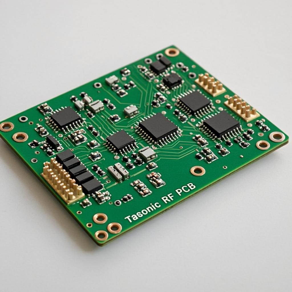
PN: B0889277A
Applications:RFID Readers, Microwave Tags, 5G IoT Modules
High frequency performance: Rogers 4350B is used for the surface layer, with a stable dielectric constant (DK=3.48 ± 0.05) and a loss tangent of only 0.0037 at 10GHz, ensuring almost zero loss transmission of microwave signals and increasing the reading distance of RFID tags to over 15 meters.
Cost optimization: The inner layer uses high TG FR-4 substrate, which reduces material costs by 30% while ensuring structural strength, making it suitable for large-scale RFID tag production.
Thermal stability: Rogers 4350B glass transition temperature (Tg)>280 ℃, FR-4 layer Tg 170 ℃, suitable for reflow soldering and extreme temperature environments.
8-layer architecture: Layers 1-2 are Rogers 4350B (antenna layer), Layers 3-6 are FR-4 (power/ground plane), and Layers 7-8 are Rogers 4350B (RF transceiver circuit), achieving perfect isolation of signal power ground.
Impedance matching: Optimize the width of microstrip/strip lines through 3D electromagnetic field simulation, support harmonic suppression up to 40GHz, and reduce the error rate of RFID systems.
Laser drilling: Minimum 0.2mm micro hole, achieving high-density interconnection and adapting to miniaturized RFID tag design.
Control deep milling groove: The antenna area adopts an isolation groove design to reduce edge radiation interference and improve reading accuracy.
Wide temperature operation: Conducted MIL-STD-202G method 107 thermal shock test (-55 ℃) ↔ 125 ℃, 1000 cycles), without delamination or foaming.
Salt spray protection: ENIG surface is resistant to salt spray for 96 hours (ASTM B117), suitable for shipborne/outdoor RFID equipment.
Anti vibration: No device detachment occurred during random vibration testing (20-2000Hz, 15Grms), meeting MIL-STD-810G standard.
Impedance Accuracy: ±5% (Standard), ±3% (Optional Customization)
Typical Impedance Values:
Single - ended Signals: 50Ω (RF Transmission Lines), 75Ω (Video Interfaces)
Differential Pairs: 90Ω (USB), 100Ω (LVDS)
Frequency Range: DC~40GHz (Supports 5G/Millimeter - Wave Applications)
Testing Methods: TDR Time - Domain Reflectometer + Vector Network Analyzer (VNA)
The surface layer uses Rogers RO4350B (DK = 3.48±0.05 @10GHz). Its stable dielectric constant ensures impedance consistency in the high - frequency band.
The inner layer FR - 4 (DK = 4.2) and the high - frequency layer are designed with a hybrid dielectric transition to optimize inter - layer impedance continuity and reduce signal reflection.
ANSYS HFSS is used to perform full - wave simulation on microstrip lines/striplines to accurately calculate the line width, spacing, and dielectric thickness:
For 50Ω microstrip lines: The line width is 0.68mm (Rogers 4350B layer)
For 100Ω differential pairs: The line width is 0.15mm/spacing is 0.2mm
It supports harmonic suppression design (e.g., the third - harmonic attenuation at 40GHz is>30dB) to reduce RF interference.
Etching Accuracy: ±0.02mm, ensuring the tolerance of the trace width.
Lamination Alignment: X - RAY positioning, with an inter - layer deviation <50μm, to avoid impedance mutations.
Surface Treatment: ENIG Electroless Nickel Immersion Gold (gold thickness 0.05 - 0.1μm), ensuring the flatness of the solder pads and reducing impedance deviations.
100% Impedance Testing: The Polar CITS900 flying - probe test system is used to conduct a full inspection of key RF networks.
Frequency - Domain Verification: The vector network analyzer (Keysight PNA) tests the S - parameters to ensure that the Voltage Standing Wave Ratio (VSWR) < 1.5 (@5.8GHz).
Environmental Reliability:
The impedance drift is <2% under high temperature (125℃) and low temperature (-40℃), meeting the MIL - STD - 883 standard.
After 96 - hour aging at 85% humidity, the impedance change rate is <3%.
Special Impedance Requirements: Supports non - standard impedance design (such as 28Ω/110Ω, etc.) and provides simulation reports and test data.
Impedance Test Report: Delivered with the board, including measured impedance values, TDR waveform diagrams, and VNA curves.
RFID Reader Antenna Feed Lines
50Ω precise matching achieves an antenna return loss of < - 20dB at 915MHz/2.45GHz, and the reading distance is increased to 15 meters.
Millimeter - Wave RF Front - End
Impedance consistency (±3%) in the 28GHz band supports millimeter - wave modules for 5G base stations and satellite communications.
High - Speed Differential Signal Transmission
The skew of 100Ω differential pairs is <5ps, ensuring the signal integrity of LVDS/USB 3.0.
Standard Basis: Complies with the IPC - 2141A impedance control specification and the IPC - 6012 Class 3A acceptance standard.
Problem Traceability: Retains impedance test data and process parameters for each batch, supporting 10 - year data traceability.
In the vast expanse of the PCB industry, Rich Full Joy has emerged as a trusted and preferred partner for our customers, thanks to a multitude of outstanding advantages. Choosing us is equivalent to injecting a powerful impetus for the success of your project. Below, we will provide you with a detailed analysis of the many key reasons why customers choose us:
A Decade of Dedicated Focus: For a full 20 years, we have been wholeheartedly committed to the field of microwave PCB manufacturing. These 20 years have been a period of continuous exploration, accumulation, and breakthroughs. We have delved deep into the characteristics of every material and every manufacturing process, achieving an industry - leading level of understanding of microwave PCBs.
Technical Strength Forged by Abundant Cases: We have successfully completed over 100 RFID projects, which cover a wide range of fields from basic applications to cutting - edge technologies. Each project has been a rigorous test of our technical capabilities, and not only have we successfully met these challenges, but we have also continuously optimized our solutions to provide customers with products and services that exceed their expectations. You can directly experience our innovative achievements and rich experience in high - frequency technology applications through our RF product line.
Lightning - Fast Delivery Speed: We deeply understand the preciousness of time during project advancement. In terms of the prototyping service for 8 - layer hybrid press boards, relying on our efficient production processes and advanced equipment, we have compressed the delivery time to ≤7 days. This means that you can obtain the samples at the earliest possible time, quickly carry out subsequent testing and evaluation work, greatly shorten the project cycle, and seize the market opportunity.
Free and Professional Impedance Test Report: To help you comprehensively understand the product performance, we provide a professional impedance test report free of charge. This report is carefully compiled by our experienced technical team, which records in detail the impedance data of the product under different environments and frequencies. It provides you with accurate data support for product design, optimization, and matching with other components, allowing you to have a clear understanding of the product quality and performance.
Comprehensive International Certification System: We have successfully passed the ISO9001 quality management system certification, establishing a scientific, rigorous, and complete quality management process. From the screening and procurement of raw materials, to every process in the production process, and then to the inspection and packaging of the final product, every link follows international standards to ensure the stability and reliability of product quality. At the same time, the UL safety certification demonstrates the excellent safety performance of our products, effectively protecting the personal and property safety of users; the ROHS environmental protection certification and the REACH regulation certification reflect our high sense of responsibility for environmental protection, and we are committed to providing customers with green and environmentally friendly PCB products.
High - Quality Presentation Under Stringent Standards: Our products strictly comply with the IPC - 6012 Class 3A standard, which represents extremely high quality requirements in the PCB industry and covers multiple key dimensions such as product appearance, dimensional accuracy, and electrical performance. Our ability to meet this standard fully demonstrates our exquisite craftsmanship and strict control in the production process, ensuring that every PCB delivered to you has military - grade excellent quality and can operate stably in various complex and harsh environments.
All - Round Customization to Meet Diverse Needs: We understand that the PCB needs of different customers vary greatly. Therefore, we provide all - round customization services from design to production. No matter what special requirements you have for the number of layers, size, or functional module layout of the circuit board, or if you need specific materials or processes, our professional team can work closely with you to tailor the most suitable solution according to the characteristics and needs of your project.
Professional Team Assisting in Solution Optimization: During the customization process, our experienced engineer team will use their professional knowledge to provide you with design optimization suggestions. By reasonably adjusting the circuit layout, selecting the most suitable materials, and other means, we can help you reduce costs and improve product performance while meeting your functional requirements, achieving the maximum benefit of the project.
Full - course Accompanied Project Follow - up: From the moment you first communicate your project needs with us, a dedicated project manager will provide you with one - on - one service. They will follow up on the project progress throughout the process and