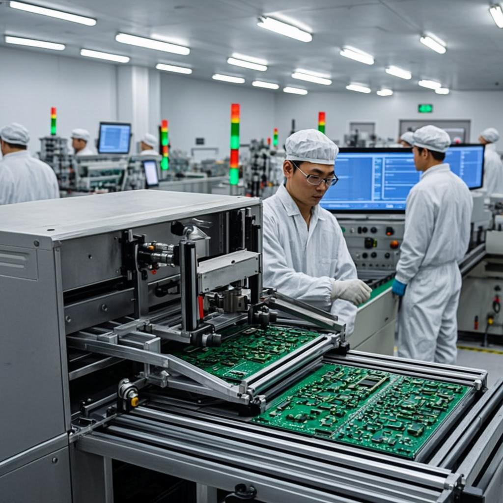
The control of lamination quality is becoming more and more important in multilayer PCB fabrication. Therefore, it is necessary to ensure multilayer laminate quality, need to have a good understanding of multilayer laminate technology. According to the processing practice for many years, Rocket PCB summarizes how to improve the laminating quality of multilayer boards as follows,
The functions of the inner laminate treatment process are as follows:
7. The organic matching of lamination parameters, the control of multi-layer board lamination parameters mainly refers to the organic matching of lamination "temperature, pressure, and time". How to determine the lamination temperature, pressure, and time software parameters is the key technology for multilayer laminate processing.
Basic material composed of the conductive pattern
A framework of the circuit board, double-sided copper clad board, which can be used for double-sided board production.
The indispensable material for multilayer board production and the adhesive between core board and core board plays an insulating role at the same time.
Various types of most commonly used FR-4 prepreg materials
Inner Layer Pre-processing
Paste Dry film Para-position Exposure Developing
Etching Strip film Inner layer AOI Lamination
After Lamination Drilling PTH Panel Plating
The purpose of the plating process is to thicken the copper thickness in the hole to prevent the hole copper from being insufficient and causing micro corrosion. The copper thickness in all holes of the working panel is 5 ~ 10 um, and the surface copper thickness is increased by 5 ~ 10 um
Pattern transfer----Exposure---Develop ( Same as inner layer process)
Pattern Plating (Plating copper and Tin)After Pattern plating After Pattern plating Strip film
Etching Strip Tin Soldermask Silksreen
Immersion Gold/Tin/Silver Routing ET/Fixture test Inspection
Package
Compared with a double-layer board, the multilayer PCB has greatly improved electromagnetic compatibility.
For example, in a four-layer board, the middle layer is used as a power layer and a ground layer, and the benefits of doing so are as follows,
it can be divided into
As mentioned above, multilayer PCB can be used in civil, industrial, and military fields. Multilayer PCB can be used for any purpose.
For many industries, multilayer PCB has become the first choice for various applications. This preference is largely due to the continuous promotion of mobility and functionality by all technologies. Multilayer PCB is a reasonable step in this process, which can reduce the size and realize more functions. As a result, they have become quite common, including:
Rocket PCB Solution Ltd is widely known as a professional PCB supplier in the electronic manufacturing industry. We have years of experience in the multilayer PCB, HDI PCB segments. Rocket PCB further expands its range of products including rigid, rigid-flex, HDI, any layer, Flex, large-size, embedded, RF, LED, backplane, the metal substrate, a ceramic substrate, IC structure, high-frequency, heavy copper. High quality and high reliability.
Get Fast Quotation
In designing Multilayer PCB, one of the most important things is to plan the stack of Multilayer PCB to achieve the best performance of the product. The bad design of the substrate and improper selection of materials will reduce the electrical performance of the signal transmission, increase emission and crosstalk, and make the product more v