Helen Frankenthaler PCB Circuit Board R&D Center

Ceramic Prototype PCB for Energy Storage

PCBMASTER Ceramic PCB Manufacturing

Ceramic PCB Manufacturing

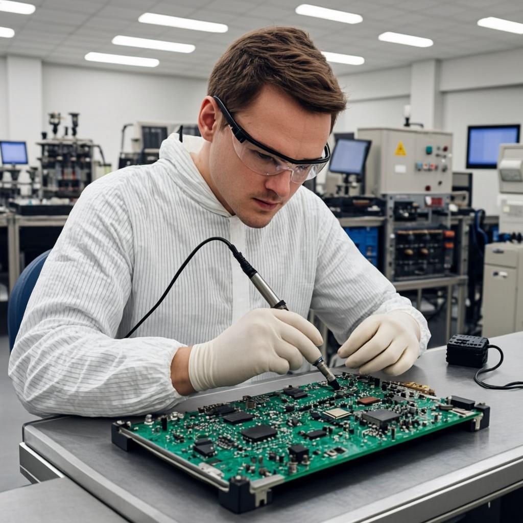
With over 10 years of R&D and production experience in ceramic substrates, we focus on tech breakthroughs for peak product performance, quality and higher production efficiency.

20 ~ 220 W/(m·K)Thermal Conductivity
< 0.03%Defective Rate
96hrs / 10-15dPrototype/Batch Urgent Order

Ceramic Substrate Product Series

Tailored for diverse scenario requirements, we offer optimized material solutions to balance performance, reliability and cost-efficiency.

The ceramic PCB materials we produce include alumina, aluminum nitride, silicon nitride, beryllium oxide (BeO), sapphire, glass, ferrite and diamond.

Different Material Comparison
MaterialThermal ConductivityInsulationToughnessCost
Alumina (Al₂O₃)20-30 W/(m·K) Sufficient for low-power devicesSuperior electrical isolationBrittle, prone to chippingLow Mature production process
Aluminum Nitride (AlN)175-220 W/(m·K) Superior heat dissipationSuitable for most electronicsLower than silicon nitrideMedium-High Higher raw material cost
Silicon Nitride (Si₃N₄)20-100 W/(m·K) Dependent on sintering processAdequate for structural applicationsHighest fracture resistanceHigh Complex manufacturing

Core Technical Advantages

From material selection to process control, every detail follows "high-reliability" standards to create industry-leading ceramic substrates.

Excellent Thermal Conductivity

Substrate thermal conductivity reaches up to 220 W/(m·K), 500-600x that of traditional FR-4, reducing component operating temperature and extending lifespan.

Extreme Temperature Resistance

Stable operation in -55℃ to 1500℃ extreme temperature ranges, meeting strict requirements of aerospace and military industries for high-temperature resistance.

Precision Circuitry

Advanced processing enables 0.05mm ultra-fine lines and 0.1mm micro-vias, satisfying high hermeticity, low outgassing and high-frequency and high-speed signal transmission needs.

CTE Matching Design

Thermal Expansion Coefficient (CTE) matches chips at 3ppm/℃, effectively reducing solder joint thermal stress and improving product reliability.

Full-process Quality Control

Compliant with AS9100, IATF16949 standards, thermal shock testing, with defect rates controlled below 0.03%.

Customized Solutions

We offer one-stop services, including material selection, structural design, SMT assembly, IC packaging and thermal simulation, to optimize performance and cost for specific scenarios.

Precision Manufacturing Capabilities

With "millimeter-level precision, micrometer-level control" as the standard, we ensure high quality through five core processes.

Layer Count1-4 Layers
Interlayer Offset0.05
Board Thickness0.2-3.0 mm
Finished Board Thickness Tolerance±0.03
Min Hole Diameter0.1 mm
Hole Diameter Tolerance±0.03
Hole Position Tolerance±0.02
Board Thickness To Hole Diameter Ratio15:1
Copper Thickness0.5-20 oZ
Copper Thickness Tolerance±20%
Min Line Width / Space0.05/0.05
Line Width Tolerance±0.015
Circuit/Solder Mask Precision±0.05
MetallizationVacuum Sputtering
Thermal Conductivity96% Alumina Ceramic: 20-27 W/m·K Aluminum Nitride (AlN) Ceramic: 180-220 W/m·K Silicon Nitride (Si₃N₄) Ceramic: ≥85 W/(m·K), Zirconia Toughened Alumina(ZTA): 20-30 W/(m·K)
Base MaterialCeramic, Sapphire, Glass, Ferrite, Diamond
Surface FinishImmersion Gold, Immersion Silver, Immersion Tin, OSP (Organic Solderability Preservative), ENEPIG (Electroless Nickel Electroless Palladium Immersion Gold)
Process TypeDPC (Direct Plate Copper), DBC (Direct Bonded Copper), LTCC (Low Temperature Co-fired Ceramic)
500,000+Annual Capacity (Pieces)
10-15 DaysStandard Lead Time
Quality CertificationsAS9100, IATF16949, ISO14001, ROHS, etc.

Application Fields

From new energy vehicles to medical devices, from 5G communication to aerospace, our ceramic substrate solutions are the core choice for high-end fields.

99% Alumina Ceramic PCB

Automotive Electronics

  • Material: 99% Alumina Ceramic PCB
  • Layers: 2 Layers
  • Thickness: 1.00mm
  • Track/Spacing: 8mil
  • Surface finish: OSP
  • Special technology: High-purity 99% alumina ceramic; High flatness of filled holes
Zirconia Toughened Alumina PCB

Medical Equipment

  • Material: Zirconia Toughened Alumina (ZTA)
  • Layers: 2 Layers
  • Thickness: 1.50mm
  • Track/Spacing: 4/4mil
  • Surface finish: Immersion gold
  • Special technology: Impedance Control +/-7%
Aluminum Nitride Ceramic PCB

5G Communication

  • Material: Aluminum Nitride Ceramic
  • Layers: 2 Layers
  • Thickness: 0.8mm
  • Track/Spacing: 4/4mil
  • Surface finish: Aluminum Nitride Ceramic Base material
  • Special technology: little Line spacing.Dimensional accuracy.IC-bonding
Alumina Composite PCB

Aerospace and Defense

  • Material: Alumina Ceramic + BT Material
  • Layers: 2 Layers
  • Thickness: 1.20mm
  • Track/Spacing: 6/6mil
  • Surface finish: Nickel-Palladium-Gold (Ni-Pd-Au)
  • Special technology: Co-fabricated Composite Process of Different Materials
Typical Customer Cases
Due to the power density of the RF module in a portable MRI device being increased to 20W/cm³, the traditional FR4 substrate (with a thermal conductivity of 0.3W/m·K) results in the chip junction temperature reaching 150℃ and thermal expansion mismatch causes solder joint cracking.
  • Material Innovation: Adopt aluminum nitride (AlN) substrates with a thermal conductivity of 170W/m·K (567 times that of FR4) and a coefficient of thermal expansion (CTE) of 4.5ppm/℃. It is highly matched with silicon chips (3ppm/℃), fundamentally solving the thermal mismatch problem.
  • Process Optimization: Achieve metallurgical bonding between ceramics and copper layers through the direct bonded copper (DBC) process, with an interface thermal resistance < 0.5℃·cm²/W. Combine with copper pillar array design to form vertical heat conduction channels, reducing the total thermal resistance to 0.15℃/W.
  • Reliability Assurance: Use active metal brazing (AMB) to enhance thermal shock resistance. After 1000 cycles of testing at -55℃~150℃, the solder joint strength retention rate is > 95%.
  • Results: The chip junction temperature is reduced to 85℃ and the power density reaches 22W/cm³. The product has passed ISO 13485 medical certification, meeting the device's 10-year service life requirement.

Blog & NEWS

1. 2. 3. 4.

FAQs About Ceramic PCB

Have more questions? Our technical team is ready to help.

Customer Reviews

Authentic feedback from clients, validating our product quality and service level.

"Our industrial power modules operate long-term in high-temperature environments above 150℃. Previously, using ordinary PCBs led to frequent thermal failures. After switching to ceramic-based PCBs, the thermal conductivity efficiency has significantly improved. They've run continuously for 6 months with zero failures, and the device temperature has dropped by 28℃ compared to before. The stability has completely exceeded expectations—truly a reliable choice for high-power applications!"

—— Mark Reynolds, Senior Power Electronics Engineer

"The core heat dissipation area of our high-end projectors has long been limited by space constraints. The thin and lightweight properties of ceramic-based PCBs perfectly fit the product design: despite a thickness of only 0.6mm, they quickly conduct heat away from the chip. This allows the projector to operate continuously for 3 hours while keeping the body temperature below 45℃. User feedback indicates a significant improvement in experience, with the repair rate dropping by 35%."

—— Emily Carter, RF Systems Engineer

"When selecting a substrate for our automotive radar module, we compared multiple options and ultimately chose ceramic-based PCBs. Not only can they withstand vibration and impact during vehicle operation, but signal transmission remains stable within the wide temperature range of -40℃ to 125℃. After 1,000 thermal cycle tests, there was no cracking or desoldering whatsoever—fully meeting automotive-grade reliability requirements."

—— David Larson, R&D Electrical Engineer