Printed Circuit Board Assembly (PCBA) is the backbone of modern electronics. From smartphones to industrial machinery, PCBAs serve as the central hub where all electronic components come together to function as a single unit. The manufacturing process of a PCBA involves meticulous planning, cutting-edge technology, and stringent quality control to ensure the final product meets the intended specifications. Here’s a detailed look at the step-by-step process of PCBA manufacturing.
The process begins with a design phase, where engineers create a schematic diagram and layout of the circuit board using software like Eagle, Altium Designer, or KiCAD. This stage involves:
Prototyping is critical as it helps identify and rectify any flaws in the design before moving to large-scale production.
The next step is fabricating the physical board, which acts as the foundation for the assembly. This involves:
Solder paste, a mix of powdered solder and flux, is applied to specific areas on the PCB where components will be placed. This is done using a stencil that aligns perfectly with the board layout. The stencil ensures that the solder paste is only applied to the pads, minimizing errors and ensuring strong connections.
Once the solder paste is applied, the board moves to the pick-and-place machine. This automated machine places surface-mount components (SMCs) like resistors, capacitors, and integrated circuits (ICs) onto the board with precision.
After the components are placed, the board is heated in a reflow oven to solder the components in place. The process involves:
This step is critical for creating reliable electrical and mechanical bonds between the components and the PCB.
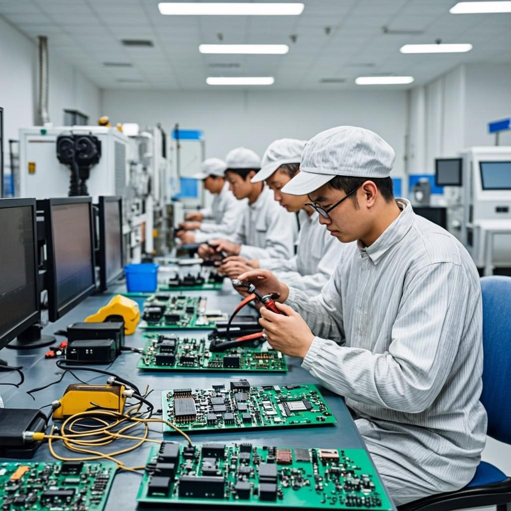
Quality assurance is paramount in PCBA manufacturing. Inspection ensures that the assembly is free of defects, such as solder bridges, misaligned components, or open circuits. Key methods include:
For boards that require through-hole components, the assembly includes:
The PCBA undergoes cleaning to remove any residues from soldering, such as flux or dust particles.
The PCBA is integrated into the final product or enclosure. This stage may involve:
Before shipment, the assembled product undergoes rigorous functional testing to ensure it operates as intended. Advanced testing equipment is used to simulate real-world conditions and verify the performance of the PCBA.
Once the PCBA passes all tests, it is carefully packaged to protect it during transportation. Anti-static materials and proper cushioning are used to prevent damage from static electricity or physical shocks.
At Zetwerk, we specialize in delivering high-quality PCBAs tailored to your specific requirements. Our manufacturing facilities in India and Vietnam offer cost-efficient solutions, ensuring compliance with global quality standards. As PCBA Suppliers in India, we provide:
Zetwerk Electronics ensures that your PCBA needs are met with precision, reliability, and a commitment to excellence.
Ready to streamline your PCBA manufacturing? Contact Zetwerk Electronics today to discuss your requirements and explore how we can help you achieve your goals.
A. A PCB (Printed Circuit Board) is the bare board without any components, while a PCBA (Printed Circuit Board Assembly) includes the board and all the components soldered onto it.
A. The timeline depends on the complexity of the design, the number of layers, and the volume of production. Typically, it ranges from a few days for prototypes to a few weeks for large-scale production.
A. Zetwerk follows stringent quality control measures, including AOI, X-ray inspection, and functional testing. We are certified to global quality standards and ensure that every PCBA meets our customers’ exacting requirements.
Contact us today to discuss your project requirements and discover how we can help you achieve your goals efficiently and effectively.