Helen Frankenthaler PCB Circuit Board R&D Center

features of pcbs 360

Multilayer PCB

Multilayer PCB: The Engine of Modern Electronics

At LHD TECH, we live and breathe the push for smaller, smarter electronics. A huge part of making that happen? Multilayer PCB Technology. It’s not just something we offer—it’s one of our core superpowers.

Think of it this way: Multilayer PCBs are how we pack more brains into less space. We take what used to require several bulky boards and engineer it into one sleek, compact unit by meticulously stacking and fusing multiple circuit layers together. This is the secret sauce behind devices that keep getting thinner, lighter, and massively more powerful.

Unlike simpler single-layer PCBs or double-sided PCBs, our multilayer tech unlocks the third dimension. We route complex, high-speed signals up, down, and through multiple insulated layers. This gives our designers incredible freedom and delivers performance that simpler boards just can’t touch.

Why are multilayer PCBs so important?

  • They’re the Innovation Engine: Think of our multilayer PCBs as the unsung heroes inside the tech that moves the world. They’re in your smartphone, critical medical gear, the data centers behind the cloud, and even satellites in space. If it’s advanced, our boards are likely at its heart.
  • Built to Handle the Tough Jobs: We engineer these boards for missions where there’s zero room for error. When a device can’t afford to be bigger, slower, or less than perfectly reliable, our PCBs are the solution.

The Secret to Smarter, Lighter Tech: This is how you pack more brains into the same space. Multilayer tech lets us cram powerful features and wireless connections into a product without making it bulkier or heavier. It’s what devices often use multilayer PCBs.

What is a Multilayer PCB?

Definition of Multilayer PCB

In our practice, a multilayer PCB is a printed circuit board by its integrated, three-dimensional structure. It is constructed by laminating three or more layers of conductive copper, each precisely separated by specialized insulating dielectric material.

This is where we leave simple boards behind. While single and double-layer PCBs work in 2D, our multilayer solutions build upward—integrating multiple circuit layers into one compact, interconnected unit. This unlocks intricate, high-density circuit design and provides the electrical stability needed for top-tier performance: think cleaner signals, controlled impedance, and much lower interference.

Key Differences Among PCB Types
PCB TypeLayer CountTypical UseComplexity
Single-Layer PCB1Simple toys, LEDs, calculatorsLow
Double-Sided PCB2Appliances, power supplies, radiosMedium
Multilayer PCB3 up to 32+Phones, computers, medical devicesHigh

Multilayer Philosophy: Building in Three Dimensions

For us at LHD TECH, the concept of a multilayer circuit board is the core of advanced electronics manufacturing. It is the engineered art of strategically stacking multiple, precise layers of conductive and insulating material into a single, high-performance system.

In our hands , we see each layer in a multilayer PCB as a step up in performance. Every sheet we add opens the door to more complexity and function, enabling advanced features—from high-speed circuitry to stable power delivery—that flat, single or double-sided boards could never handle.

This multidimensional mindset is how we take a simple board and evolve it into the integrated, high-powered core of tomorrow’s tech.

Multilayer PCB Structure & Architecture

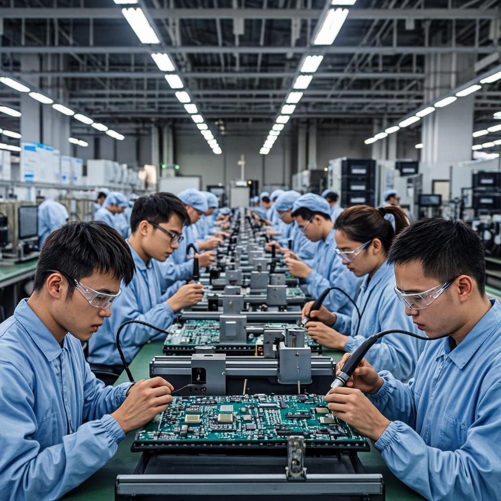
At LHD TECH, we engineer a multilayer PCB consists of layers of the multilayer PCB system. We meticulously arrange and permanently bond its individual layers under heat and pressure to form a single, compact, and exceptionally reliable assembly. Each stratum in this stack has a distinct purpose, working in concert to provide optimized paths for signal transmission, efficient power distribution, and integral mechanical support.

Layers of the Multilayer PCB
  1. Outer layers of the board– These are the surfaces of the board, engineered for reliable component mounting and external interconnection.
  2. Inner layer core–The heart of complexity. These middle layers are dedicated to routing critical signal traces, establishing robust power planes, and creating continuous ground planes for stability and noise suppression.
  3. Layer of conductive material– The circulatory system. Every functional layer incorporates precisely etched copper traces that form the essential circuit pathways for electrons to flow.
  4. Prepreg/Insulator– The essential isolation. This insulating material is laminated between each copper layer, preventing electrical shorts and defining the board’s critical electrical characteristics.
  5. Soldermask– The protective skin. Applied over the outer layers, this coating prevents accidental shorts during assembly and shields the copper from corrosion and environmental damage.
  6. Outer layers of the board– The functional guide. This final printing provides component designators, orientation markings, and logos, ensuring accurate and efficient assembly.
Multilayer PCB Architecture Diagram
Layer NameMain FunctionExample Use
Top LayerComponents/SMD, testMounting chips, interface pads
Signal LayerRouting signalsHigh-speed buses, clocks
Power PlanePower distributionVCC, core voltage supplies
Ground PlaneEMI controlCommon reference for signals
Bottom LayerComponents, connectorsDIP, edge connectors
Why Multilayer is the Right Choice?

Our multilayer technology grants designers the power to:

  1. Manage High-Density Layouts: We pack more functionality into a smaller footprint, essential for today’s miniaturized devices.
  2. Implement Advanced Isolation: We enable the clear separation of analog and digital grounds, a fundamental requirement for preventing noise and ensuring signal purity.
  3. Provide Integrated Shielding: Sensitive traces can be shielded between solid ground planes, dramatically reducing interference and crosstalk.

This combination of capabilities makes the use of multilayer PCBs from LHD TECH not just beneficial, but essential. They are the enabling platform for high-performance applications in RF and wireless communications, sophisticated power management systems, and complex mixed-signal processing devices where signal integrity is paramount.

Types of Multilayer PCBs and Layers

Multilayer PCBs can be divided by the number of conductive layers as well as the type of construction, whether standard rigid, dynamic flexible multilayer PCB, or integrated rigid-flex.

Common Multilayer PCB Types
  • 4-layer PCB:Our go-to solution for basic digital or analog devices. LHD TECH optimizes the layer stack-up (typically Signal-Ground-Power-Signal) to provide a perfect balance of performance, simplified EMI management, and cost for a wide range of consumer and industrial products.
  • 6-layer PCB:We frequently recommend this configuration for embedded applications and advanced microcontroller systems. By designing dedicated internal power and ground planes, our engineers effectively isolate sensitive signals, significantly reducing noise and crosstalk for more stable and reliable operation.
  • 8+ layer PCB:When performance is non-negotiable, LHD TECH delivers high-layer-count boards essential for high-frequency communication, server motherboards, and advanced computing. Our expertise in sequential lamination and precise impedance control ensures signal integrity in the most demanding RF and high-speed digital environments.
Specialty Multilayer PCBs

We push boundaries with advanced materials and hybrid constructions:

  • Flexible multilayer PCB:Our engineering enables innovation in space-constrained and dynamic applications. We manufacture reliable multilayer flex circuits for foldable devices, advanced camera systems, and critical aerospace instrumentation, where repeated bending is required without sacrificing connection density.
  • Rigid-flex multilayer PCB:At LHD TECH, we master the art of combining rigidity and flexibility. By integrating rigid boards for component support with flexible interconnects, we create seamless, highly reliable 3D assemblies perfect for miniaturized medical implants, wearable health monitors, and ruggedized defense electronics.
  • Backplane and Embedded boards:For the backbone of network infrastructure and miniaturized sensors, we design complex backplanes for communication switches and embedded boards with microvias and embedded passive components. This maximizes functionality while minimizing size and weight.
Applications of Multilayer PCB Structures

The applications of multilayer PCBs are virtually limitless. We provide the essential platforms that enable cutting-edge technology:

  • Complex beamforming and signal processing in 5G/6G antenna systems.
  • Compact, energy-efficient LED drivers and smart lighting controllers.
  • Dense, reliable circuitry for next-generation smart wearables and IoT edge devices.

Where standard boards fall short, LHD TECH’s multilayer pcbs are used the performance, density, and reliability your innovation demands.

Types of Vias in Multilayer PCBs

At LHD TECH, we understand that the intelligence of a multilayer PCB lies not just in its layers, but in the sophisticated interconnections that bind them. Selecting the right via technology is fundamental to achieving signal integrity, reliability, and density in our advanced designs.

We deploy blind and buried vias structures to optimize performance and manufacturability for every project:

  • Through-Hole Via:Our foundational solution. This via passes through the entire board stack-up, providing a robust and reliable connection from the top to the bottom layer. It is essential for power connections, mounting through-hole components, and designs where cost-effectiveness is paramount.
  • Blind Via:A key enabler for high-density designs. Engineered by LHD TECH, this via connects an outer layer to one or more inner layers without traversing the entire board. This conserves valuable routing space on layers it does not reach, allowing for more compact and efficient component placement, such as under fine-pitch components.
  • Buried Via:For maximum internal routing efficiency. Completely encapsulated within the inner layers, our buried vias connect only internal layers without reaching either outer surface. This technology is critical for complex, high-speed digital boards, allowing additional signal routing channels between power planes while maintaining a pristine outer layer landscape for component mounting.
  • Microvia:The cornerstone of our High-Density Interconnect (HDI) capability. These laser-drilled, ultra-small vias (typically <150µm) are essential for escaping modern, high-pin-count Ball Grid Array (BGA) packages and enabling advanced stacked and staggered via structures. LHD TECH leverages microvias to achieve the miniaturization and performance required in cutting-edge consumer, medical, and communication devices.

How Do Multilayer PCBs Work?

To us, a multilayer PCB is more than just materials—it’s a fully engineered electronic ecosystem. By bonding multiple conductive and insulating layers into one compact structure, we achieve three key things: dramatically higher circuit density, smarter functional integration, and electrical performance that simple boards can’t touch.

Key Principles

Our multilayer designs are governed by these key engineering principles to guarantee functionality and reliability:

  • Separated Signal Paths:We give critical signals their own dedicated routes—either on separate layers or in controlled channels. This isolation slashes crosstalk and electromagnetic interference, guaranteeing clear, high-fidelity signal transmission.
  • Optimized Power Integrity:We build in dedicated power and ground planes designed for low impedance. This ensures rock-solid voltage delivery across the entire board, eliminating dips and noise that can degrade both digital and analog performance.
  • Proactive EMI Control: Our strategic use of solid internal ground planes acts as highly effective shielding. This containment of electromagnetic fields is critical for the stability of sensitive analog, RF, and mixed-signal circuits.
  • Heat management:We engineer thermal performance directly into the stack-up. From using heavy copper layers to integrating metal cores or thermal vias, our designs efficiently dissipate heat from high-power components, ensuring long-term system reliability and performance.

Key Advantages of Multilayer PCBs

Benefits of Using Multilayer PCBs

We’re not just building PCBs—we’re engineering smarter systems. Every multilayer board we create is designed to bring real performance gains and rock-solid reliability. That’s why our technology is the foundation behind better, next-level electronics.

The LHD TECH Multilayer Advantage: Key Benefits for Our Clients

  1. Space and Weight Reduction

At LHD TECH, we focus on doing more with less. We design with higher circuit density to create smaller, lighter boards that pack more punch into every square millimeter. This is especially vital for our partners in wearables, mobile tech, and aerospace, where every fraction of a gram and every sliver of space truly matters.

  1. Superior Electrical Performance

We engineer for speed and signal integrity. Our multilayer