Printed Circuit Board (PCB) assembly and soldering are fundamental processes in electronics manufacturing. This guide covers the essential steps and considerations for creating reliable electronic assemblies.
The assembly process typically follows a sequence to ensure accuracy and quality.
Solder paste, a mixture of tiny solder balls and flux, is precisely applied to the PCB pads using a stencil.
Surface Mount Technology (SMT) components are placed onto the solder paste by a pick-and-place machine or manually for prototypes.
The board passes through a reflow oven. The heat melts the solder paste, creating permanent electrical and mechanical connections.
Leaded components are inserted into designated holes on the PCB.
For through-hole parts, the board's underside passes over a wave of molten solder or solder is applied selectively to each joint.
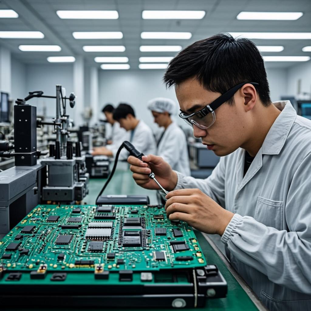
Assembled boards undergo visual inspection, Automated Optical Inspection (AOI), and functional testing.
Effective soldering is crucial for strong, conductive joints.
For rework and prototyping, hand soldering with an iron is common.
Understanding potential issues helps in achieving higher yield.
Unintended connections between adjacent pins or pads. Prevent by using correct solder paste volume and accurate stencil alignment.
A component stands up on one end during reflow. Caused by uneven heating or pad design. Ensure symmetric pad layout and thermal mass.
Dull, grainy joints that are weak and poorly conductive. Caused by insufficient heat. Ensure the iron or oven reaches proper temperature and heating time.
Flux residues can be corrosive. Clean boards after soldering, especially for high-reliability applications, using appropriate solvents or aqueous cleaners.
Mastering PCB assembly and soldering requires attention to detail, proper materials, and controlled processes. Whether for large-scale production or hobbyist projects, following best practices ensures the creation of functional and durable electronic devices.