Helen Frankenthaler PCB Circuit Board R&D Center

FR4 Long PCB for Smart Home

Smart Home PCB: Design, Applications & Trends

What is a Smart Home PCB?

A Smart Home PCB (Printed Circuit Board) is the foundation that powers most modern smart devices in our homes. Think of it as the “brain” that connects and controls everything from your smart lights to your security camera. By embedding microcontrollers, sensors, and communication modules, Smart Home PCBs allow devices to communicate, process data, and execute commands reliably. Without them, the seamless operation of connected devices in a smart home wouldn’t be possible.

Role in IoT and Home Automation

In today’s IoT-driven world, Smart Home PCBs play a central role in home automation. They act as the hub where devices like thermostats, cameras, and entertainment systems connect, ensuring smooth data exchange and remote control. Whether it’s scheduling your lights to dim at night or checking your front door camera while you’re away, Smart Home PCBs make these automated experiences possible.

Benefits of Smart Home PCBs

Smart Home PCBs don’t just add convenience—they also bring multiple benefits that transform everyday living:

  • Connectivity: Seamlessly link multiple devices across the home.
  • Automation: Simplify routines with pre-set schedules and triggers.
  • Energy Efficiency: Optimize power use and cut down unnecessary consumption.
  • Security: Strengthen safety with integrated sensors and smart locks.

In short, Smart Home PCBs are the invisible backbone that powers the smarter, safer, and more efficient homes we enjoy today.

Applications of Smart Home PCB

Smart Home PCBs are everywhere in modern houses—even if you never see them directly. They sit inside your favorite devices and quietly handle the automation, connectivity, and control that make a smart home truly “smart.” Let’s explore the main ways they are used:

  • Lighting control: PCBs allow you to dim lights, change colors, and set schedules. This not only saves energy but also creates the perfect atmosphere for any moment.
  • Security systems: From smart cameras to motion sensors and digital locks, PCBs help you keep your home safe. They enable remote monitoring, instant alerts, and stronger protection.
  • Thermostat & HVAC control: Heating and cooling become smarter with PCBs. They let you adjust settings remotely, schedule temperature changes, and cut energy waste.
  • Entertainment systems: TVs, speakers, and media hubs run smoothly thanks to PCBs. They provide reliable connections, better sound quality, and a more enjoyable home entertainment experience.
  • Home automation hubs: These act as the central brain of a smart home. PCBs link all devices—lighting, security, heating, and entertainment—into one system you can control from your phone or voice assistant.
  • Sensor-based applications: Smart Home PCBs work with sensors to monitor temperature, humidity, smoke, and air quality. This improves comfort, safety, and awareness of your living environment.

Key Components of Smart Home PCB

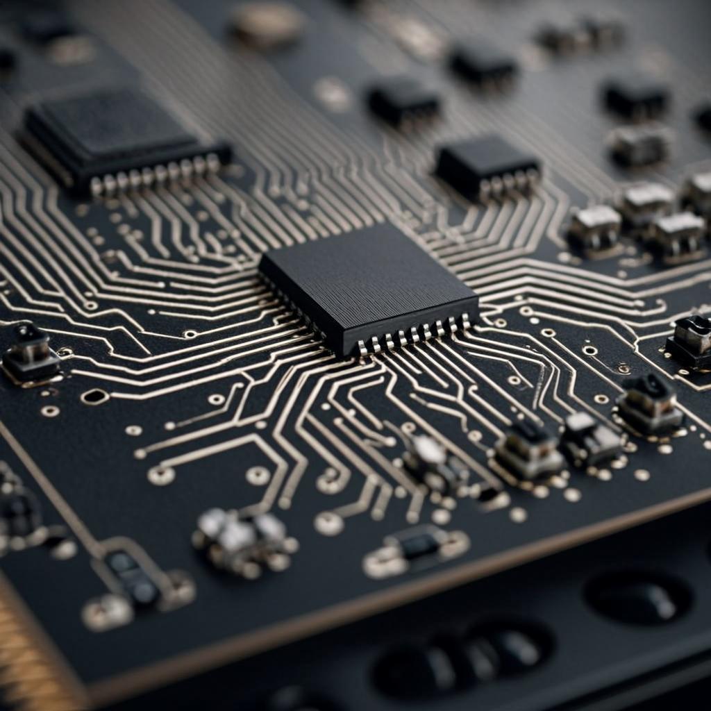
Every smart device relies on a Smart Home PCB to bring its features to life. Let’s look at the main components that make these boards work:

  • Microcontroller / Processor: Often called the brain of the device, this chip processes data, runs commands, and manages communication between all parts of the system.
  • Sensors: These collect real-time data such as temperature, motion, humidity, or smoke levels. They help devices respond to changes in the environment and keep your home safer and more comfortable.
  • Connectivity modules: Technologies like Wi-Fi, Bluetooth, and Zigbee allow devices to connect to each other and to your smartphone or central hub. Without these, smart home automation wouldn’t be possible.
  • Power management: Voltage regulators and low-power designs ensure that devices run efficiently, avoid overheating, and extend battery life.
  • Memory & storage: Components such as RAM and flash memory keep essential data, settings, and user preferences stored, ensuring smooth operation.
  • Interfaces & ports: Everyday interactions happen here, whether it’s a USB port, touchpad, or button. These give users simple ways to control and connect with their devices.
  • Actuators: These components turn signals into actions, like opening a smart lock, moving a motor, or switching on a fan.

Smart Home PCB Design & Manufacturing Workflow

Designing and producing a Smart Home PCB is a step-by-step process that turns an idea into a working device. Each stage is important to make sure the final product is reliable, efficient, and ready for everyday use.

Device analysis & requirements gathering

The process starts with understanding the device’s purpose. Will it control lighting, monitor security, or manage energy? At this stage, engineers identify the right sensors, processors, and connectivity modules needed for the design.

Prototyping and conceptualization

Before going into full production, a prototype is built to test features and functions. This step helps confirm that the chosen components and design will actually work in real-world conditions.

Schematic design and PCB layout

Once the idea is validated, engineers create a schematic, or blueprint, that shows how each component connects. Tools like Altium, Eagle, or KiCAD are used to design the PCB layout, focusing on signal integrity, power distribution, and compact size.

Fabrication & assembly

With the layout finalized, it’s time to build. The fabrication stage creates the physical board, while assembly adds the components. Techniques like SMT (surface mount technology), pick-and-place machines, and soldering ensure precise and efficient production.

Testing & inspection

Every board must pass rigorous testing. Engineers check for signal accuracy, durability, and overall quality to make sure the PCB meets performance standards before moving forward.

Firmware programming & integration

Finally, the board is loaded with firmware, the software that allows the PCB to communicate with devices and users. This step brings the smart home system to life, enabling automation, connectivity, and remote control.

Challenges in Smart Home PCB Design

Building a Smart Home PCB isn’t always simple. Designers face several challenges when creating boards that need to be compact, powerful, and reliable all at once.

  • Miniaturization: Smart devices are getting smaller, which means PCBs must fit more components into less space. Using HDI (High-Density Interconnect) techniques, multilayer boards, and careful heat dissipation methods helps achieve this. The challenge is packing everything in without sacrificing performance.
  • Power efficiency: Since smart home devices often run continuously, they need to be designed with low-power components and dynamic power scaling. A poorly optimized design can lead to excessive heat, wasted energy, and shorter device lifespans.
  • Signal integrity & EMI: With so many interconnected devices, electrical signals must remain stable. Designers need to manage controlled impedance, proper grounding, and shielding to prevent interference. Without this, issues like data loss or poor connectivity can occur.
  • Balancing compact size with reliability: Shrinking the PCB is important, but it can’t come at the cost of durability. The real challenge is to design boards that are both compact and strong enough to handle long-term use in demanding home environments.

Future Trends in Smart Home PCBs

The world of Smart Home PCBs is evolving quickly, and new technologies are shaping how our devices will look and perform in the coming years. Here are some of the most exciting trends to watch:

  • Miniaturization & integration of more functions: Devices are getting smaller and sleeker, yet they need to do more. Future PCBs will integrate multiple functions into compact boards without losing performance.
  • Advanced sensors for environmental monitoring: Expect smarter PCBs that include sensors to track temperature, humidity, air quality, and smoke. These features will make homes safer and more energy-efficient.
  • Gesture and touch-sensitive user interfaces: Instead of relying only on apps or remotes, future PCBs will support direct touch and gesture controls, creating smoother, more natural interactions with devices.
  • AI & machine learning integration: On-board intelligence is becoming a reality. Smart Home PCBs will soon include AI chips that allow devices to learn user habits, make faster decisions, and even predict needs.
  • Sustainability: With a growing focus on the environment, manufacturers are moving toward eco-friendly PCB materials and greener production processes. This ensures smarter homes are also more sustainable.
  • Scalability & modular design: Homes will continue adding more devices, so PCBs will be designed with modular structures that make upgrades and expansions easier.

FAQs About Smart Home PCBs

What are Smart Home PCBs used for?

Smart Home PCBs are used in devices like lighting systems, thermostats, security cameras, and automation hubs. They connect sensors, processors, and communication modules, making it possible for smart devices to interact and work together.

How do Smart Home PCBs improve energy efficiency?

By using low-power components and optimized power distribution, Smart Home PCBs help reduce wasted energy. Features like scheduling lights or adjusting heating and cooling automatically also cut down on unnecessary power use.

What challenges do designers face with Smart Home PCBs?

The main challenges include miniaturization, power efficiency, and signal integrity. Designers need to fit more functions into smaller boards while keeping them reliable, energy-efficient, and free from interference.

Can Smart Home PCBs support AI and IoT integration?

Yes. Modern Smart Home PCBs are built with connectivity modules and AI-ready chips, allowing devices to connect through IoT networks and even learn user habits for smarter automation.

How to choose the best Smart Home PCB manufacturer?

Look for a manufacturer with experience in IoT devices, strong certifications (ISO, UL), advanced capabilities like multilayer and HDI boards, and rigorous testing processes. Good communication and reliable supply chains are also key.

Conclusion

Smart Home PCBs play a key role in today’s IoT-driven homes. They make devices more connected, smaller, and energy-efficient, while ensuring safety and convenience. As technology advances, these boards will only become smarter and more reliable.

To get the best results, it’s important to work with a trusted partner. GlobalWellPCBA offers professional PCB design and assembly services for smart home products. Contact us today to see how we can help bring your ideas to life.

  • Comprehensive Guide to PCB Design and Basics
  • HVAC Circuit Board: How It Works & Why It Matters
  • FPGA vs Microcontroller: Key Differences Explained
  • What is a PIR Sensor? Working, Applications & Benefits
  • What is electr