Compact IoT controllers now combine MCU, wireless, sensors and power management on very small PCBs. As board size shrinks, routing congestion, fine-pitch BGAs, dense power pins, and RF constraints quickly push traditional 2- or 4-layer designs to their limits.
Compact HDI PCB integrating MCU, wireless module and power management in a space-constrained IoT design
HDI PCB technology solves these density challenges using microvias and optimized stackups to enable clean signal escape and stable power delivery. This article walks through a practical, step-by-step project showing how HDI turns a constrained IoT layout into a production-ready design.
In this project, we are designing a 50 mm × 40 mm compact IoT controller intended for industrial monitoring and smart infrastructure applications. The board must collect sensor data, process it locally and transmit it wirelessly — all within a single compact PCB.
We are not designing a simple sensor node. The board must integrate:
IoT Controller System Block Diagram: Functional architecture of the compact IoT controller before PCB layout begins
On a standard 4-layer board, routing under the MCU quickly becomes congested. Power pins cluster tightly. RF routing demands clean impedance control and antenna isolation. Simply adding layers increases cost but does not fix breakout congestion.
To make this board manufacturable and reliable, we will:
This project will walk through each of these decisions step by step — from constraints to placement, stackup, fanout, routing and DFM validation.
Before placing a single component, we lock the constraints. In compact IoT projects, most redesigns don’t happen because traces were routed badly — they happen because requirements weren’t fixed early.
For this controller, we define three hard boundaries: electrical, mechanical, and manufacturing.
This board must support:
These requirements immediately increase:
This tells us early: a simple multilayer board will likely struggle.
50x40mm IoT PCB Mechanical Constraints: Mechanical and placement constraints fixed before routing begins
The enclosure fixes the board size at 50 mm × 40 mm. Connectors and antenna position are pre-defined. Component height is limited.
We cannot:
This removes traditional layout escape options.
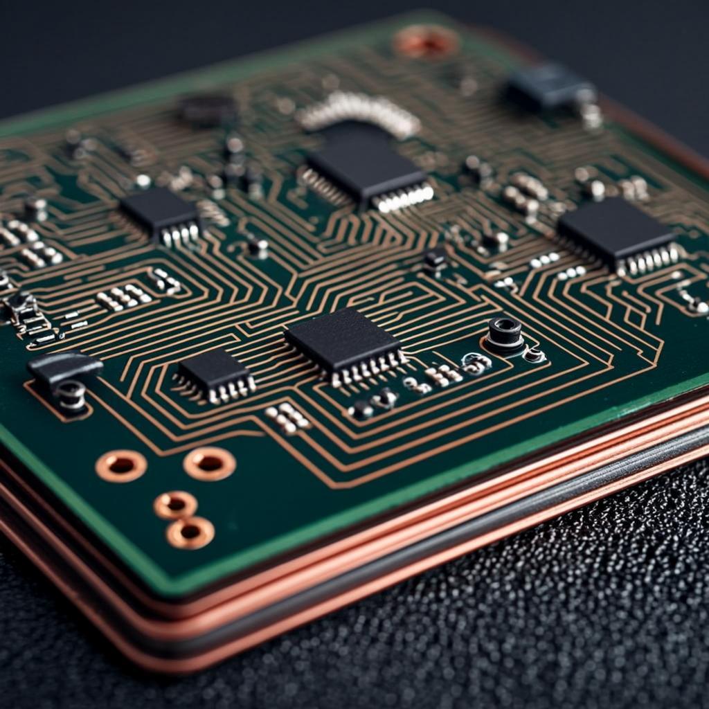
Once the project constraints were locked, the next major decision was stackup selection. In a compact 50 × 40 mm IoT controller, stackup determines whether BGA fanout will route cleanly, whether RF signals will maintain a stable reference, and whether power delivery will remain reliable during wireless transmission peaks.
Early evaluation showed that a 2-layer or standard 4-layer board could not support dense MCU breakout or controlled RF routing. Even a conventional 6-layer stackup struggled because through-hole vias consumed too much escape space under the fine-pitch package.
1+4+1 HDI PCB Stackup Structure: The 1+4+1 stackup enables clean BGA fanout and stable reference planes
Image File name - 1-4-1-hdi-pcb-stackup-structure
To solve this without over-engineering the board, the design adopted a 1+4+1 HDI stackup. This structure enables direct microvia fanout from the MCU, keeps signal layers tightly coupled to solid ground planes, supports low-inductance power delivery, and maintains mechanical symmetry for reliable assembly. Microvias are limited to adjacent layers only, with no stacking, keeping fabrication practical and scalable. The result is the simplest HDI configuration that eliminates routing congestion while remaining production-friendly.
In this project, we quickly realized that routing would not decide success—placement would. In compact IoT controllers, poor placement can increase layer count, force aggressive microvia usage, and create signal integrity problems that no routing trick can fix later. So before drawing a single trace, we treated placement as the most critical engineering step.
Insert Image 4 Here
Alternative Text - MCU centered placement with wireless module near edge and organized power section in HDI IoT PCB
Caption - Strategic placement reduces routing congestion before fanout begins
Image File name - hdi-iot-pcb-component-placement-strategy
The MCU was placed first and positioned near the center of the PCB. This provided balanced routing access on all four sides and allowed microvias to escape cleanly into adjacent layers. Placing it near the edge would have immediately restricted breakout channels and increased stackup complexity. The wireless module was locked early as well, positioned near the board edge with a defined antenna keep-out zone. This prevented RF compromises later and avoided the common mistake of trying to fix antenna performance during routing.
Sensors and interfaces were grouped logically based on signal flow rather than convenience. Devices communicating directly with the MCU were kept physically close to reduce trace length and noise exposure. The power section was placed with current flow in mind—regulators close to their loads, decoupling capacitors directly at MCU power pins, and high-current loops kept tight and localized.
By the time routing began, the board already felt organized and predictable. That was intentional. In compact HDI designs, clean placement reduces routing stress more effectively than adding layers or increasing via complexity.
In this project, HDI was used to solve routing congestion under a fine-pitch MCU BGA. The goal was controlled routing — not maximum density.
Fine Pitch BGA HDI Routing Closeup: Microvia-based fanout reduces congestion under fine-pitch BGA packages
At this stage, routing is complete—but before fabrication, the design must be validated from a production and reliability standpoint. In compact HDI IoT controllers, most field failures are not caused by schematic errors. They originate from power instability, broken reference planes, or RF layout weaknesses that were not caught before manufacturing.
This step ensures the design is not only functional — but production-stable.
Before release, we verify:
Critical checks include:
Validation focuses on:
Power Integrity RF Routing HDI PCB: Continuous ground reference protects RF performance and reduces EMI
Before Gerber release, the design should confirm:
In practice, early collaboration between design teams and experienced HDI manufacturers such as NextPCB helps validate stackup feasibility, via strategy, and electrical assumptions before fabrication begins. This alignment significantly improves production predictability and reduces redesign cycles.
At this stage, the PCB is electrically complete — but not yet production-ready. Many HDI boards that pass ERC and DRC still fail during fabrication because design limits were pushed beyond practical manufacturing capability. This step converts the layout into something that can be built reliably and repeatedly.
HDI PCB Microvia Features DFM:Manufacturing limits define reliable HDI microvia implementation
HDI features are reviewed against proven process capabilities:
This prevents common HDI risks such as solder wicking, voiding, alignment sensitivity, and yield instability.
The selected 1+4+1 stackup is checked against actual fabrication flow: