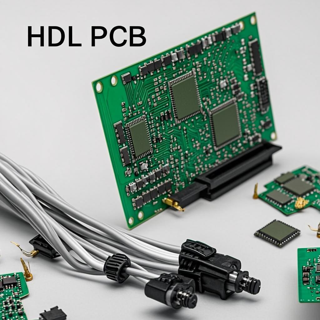
A 20 layers HDI PCB (High-Density Interconnect Printed Circuit Board) is a 20-layer PCB that utilizes microvia technology to achieve high-density wiring. Its features include smaller line widths/spacings (typically ≤75μm), buried and blind via structures, high integration density, and low signal loss. Compared to traditional multilayer PCBs, 20 layers HDI PCB offer superior electrical performance, space utilization, and reliability, and are widely used in high-end fields such as 5G communication, medical equipment, aerospace, and consumer electronics.
A detailed design guide 20 layers HDI PCB board:
Layer Allocation Principle:Adopt an alternating “signal layer + plane layer” structure. Recommend 10-12 signal layers + 8-10 plane layers (power/ground). Example: Top signal layer, GND layer, signal layer, VCC layer, signal layer, GND layer… Bottom signal layer.
Symmetry Design:Ensure mirror symmetry of layers (e.g., layer 3 matches layer N-2) to prevent board warpage. Layer stack thickness must align with copper thickness (e.g., 50-100μm dielectric thickness for 18μm copper).
Material Selection:Use low-loss substrates (e.g., Panasonic M6/M7) for high-frequency applications; standard FR-4 suffices for general cases. Inner layers should use low dielectric constant (Dk) materials to minimize signal delay.
Via Type Selection:Prioritize laser-drilled blind/buried vias (diameter ≤100μm) to reduce through-hole ratios. Example: 1st-order HDI uses 1+N+1 structure (top blind via → inner layer); 2nd-order HDI uses 2+N+2 structure (top blind via → inner buried via → bottom).
Via Dimensions:Minimum via size must match manufacturing capabilities (typically ≥75μm), with spacing ≥100μm. Blind vias should be staggered to avoid stress concentration.
Plating Process:Use electroless copper + electroplating to achieve >80% via fill ratio, preventing voids that compromise reliability.
Impedance Control:All signal layers require strict impedance design (single-ended 50Ω±10%, differential 100Ω±10%). Calculate trace width/spacing using tools like Polar SI9000, accounting for substrate Dk and copper roughness.
Crosstalk Mitigation: Sensitive signals (e.g., high-speed differential pairs) follow the 3W rule (trace spacing ≥3x trace width). Add ground shielding traces if necessary. Differential pairs must match lengths (error ≤5mil); inner-layer pairs prefer stripline structures.
Return Path Planning:Ensure high-speed signals have continuous reference planes (ground or power) beneath them, avoiding plane splits. Critical signals (e.g., clocks) should route in inner layers to reduce radiation.
Power Plane Partitioning: Segment power planes by module (e.g., CPU core voltage, I/O voltage) to prevent plane fragmentation. Use anti-pads to control copper-to-via clearance (typically ≥20mil).
Decoupling Capacitor Placement:Position high-frequency decoupling caps (0.1μF) near chip power pins; place bulk caps (≥10μF) at power entry points. Route caps with minimal loop area using the “closest principle.”
Power Plane Thickness:Recommend ≥2oz (70μm) copper for power layers to lower impedance; widen copper traces or use copper bars for high-current paths.
Heat Dissipation Design: Add thermal vias (via farms) beneath high-power devices (e.g., BGA packages) to form heat channels. Use inner thermal layers and high-thermal-conductivity substrates (e.g., TGF).
Thermal Via Arrays: Densely arrange thermal vias (spacing ≤1mm) in heat-source areas. Fill vias with thermal paste or copper paste to enhance heat transfer.
Temperature Monitoring:Reserve thermistor pads in critical zones; design considering airflow paths to prevent heat buildup.
Trace/Space Dimensions:Minimum trace width/spacing ≥3mil (matching manufacturing capabilities). Use negative-tone processes in dense areas to reduce etching defects.
Soldermask and Marking:Soldermask openings must exceed pads by 10μm to avoid bridging; ensure clear silkscreen markings without covering test points.
DFM Checks:Use tools like Allegro or Altium for DRC/DFM validation, focusing on: minimum via size/spacing, impedance matching, copper connectivity, and thermal via placement.
Test Point Design: Reserve test points (spacing ≥100mil) for critical signal pins using test fixtures or flying probes.
Simulation Validation:Perform SI/PI simulations (e.g., HyperLynx, ADS) to identify reflections, crosstalk, or ground bounce early.
Prototype Verification:After fabricating engineering samples, conduct electrical tests, thermal imaging, and mechanical tests (e.g., thermal shock, vibration) to validate design compliance.
20-Layer HDI PCB Production Process:
Reasons to choose EBest Circuit (Best Technology) for 20 layers HDI PCB manufacturer:
Cost-Competitive Pricing with 15-20% Savings: Benchmarked against industry averages, our pricing model delivers 15-20% cost savings without compromising quality. For a 20-layer HDI prototype, customers report average savings of 800−1,200 per batch compared to Tier-1 competitors.
99.8% Yield Rate: Strict process controls (ISO 9001:2015/ISO 14001 certified) and automated optical inspection (AOI) systems ensure <0.2% defect rate. Our 100% electrical testing protocol eliminates open/short defects, backed by a 2-year warranty for volume orders.
Impedance Testing with ±5% Accuracy: Every 20-layer HDI board undergoes Time-Domain Reflectometry (TDR) testing with Polar Instruments SI9000. Our impedance control meets IPC-6012 Class 3 standards, with single-ended 50Ω±5% and differential 100Ω±5% tolerance.
19-Year Expertise in 20-Layer HDI Manufacturing: With 19 years of specialized HDI experience, we’ve delivered over 120,000 20-layer boards for 800+ global clients. Case studies show 30% shorter design cycles and 40% higher first-pass success rates for complex HDI projects.
Free DFM Analysis Saving 30% Design Time:Complimentary Design-for-Manufacturing checks using Siemens Xpedition identify 50+ potential issues (e.g., via spacing, trace width). Clients report 30% reduction in design iterations and 50% faster time-to-market.
72-Hour Rapid Prototyping with 99.2% On-Time Delivery:Our accelerated workflow delivers 20-layer HDI prototypes in 72 hours – 40% faster than indus