High-Density Interconnect (HDI) printed circuit boards are an advanced design of circuit board, designed to support significantly higher wiring density per unit area than standard PCBs. HDI boards use microvias, fine traces and high layer counts to make electronic devices smaller, lighter and more powerful.
HDI PCB technology is now widely used in smartphones, medical devices, automotive electronics and aerospace systems, as it can deliver the miniaturisation and signal integrity demanded by these applications.
A circuit board that has more wire per unit area than a typical board is referred to as an HDI PCB. The design may use thinner lines and gaps, smaller vias and capture pads, and greater connection pad densities since HDI PCBs have a higher circuit density.
Your device’s overall enactment can be considerably improved by using an HDI rather than a regular PCB.
The dependability of your board and your goods can be increased by the reduced aspect ratios and the premium micro via structure.
The ability to secure more components on both sides of the bare PCB using HDI boards enables you to squeeze more functionality into a smaller area and increase the equipment’s overall capabilities. You may increase functionality while making your goods smaller and lighter thanks to HDI technology.
An increase in the number of transistors and a reduction in the distance between components can result in better electrical performance. Microvia technology enables circuit board designers to reduce radio frequency interference and electromagnetic wave interference by shortening the distance between the ground layer and the signal layer. Lower power consumption is made possible by these qualities, which enhances signal integrity.
HDI boards can be more economical than other solutions with careful design and production since they use less raw materials because of their compact size and few required layers. You might be able to employ one HDI board for a product that previously would have needed several conventional PCBs. More functionality and value may be obtained with a smaller footprint and less material.
Faster manufacturing speeds and a quicker time to market can result from the capacity to utilize less resources, and even fewer boards, in combination with design savings tied to HDI technology. Due to the superior electrical performance and relatively simple component placement, HDI PCBs require less time to test and debug.
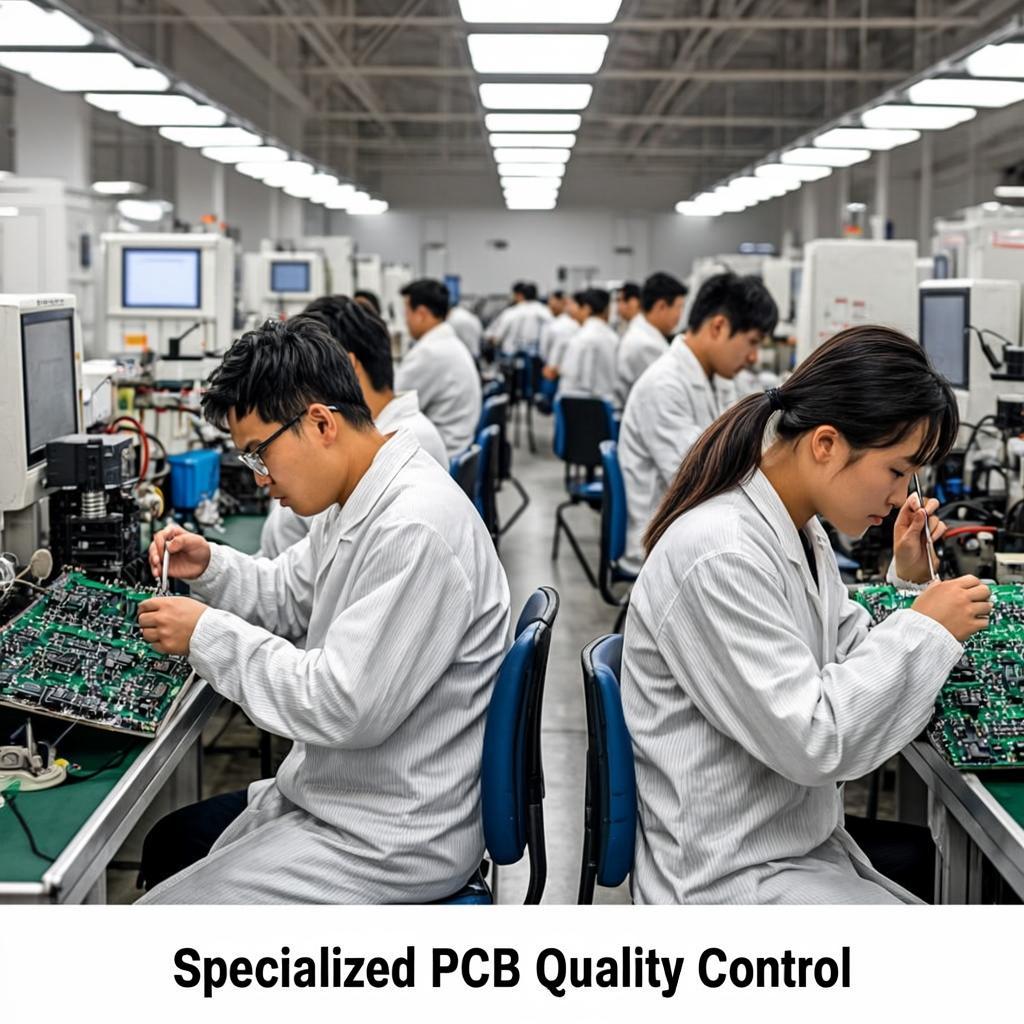
Although HDI PCB manufacturing is similar to standard PCB production, it involves greater precision and more advanced processes. When dependability needs are taken into account, DFM requirements also become significant.
The details of HDI PCB fabrication are provided as follows:
Although HDI PCB processing techniques are more complex than conventional rigid PCB processing procedures, they nonetheless employ the same manufacturing data as a standard rigid PCB. Deliverables for your manufacturer should be ready after your HDI PCB design is done and has passed a DFM review.
One of the areas of the printed circuit board industry with the quickest growth is HDI PCBs.
Since HDIs are compact and easily fit in implants and imaging equipment, they are being incorporated into the majority of medical devices like:
Manufacturers of automobiles and other vehicles are drawn to HDI PCBs because they enable a great deal of creativity. With HDI PCBs, you may boost a vehicle’s performance while saving more room. They’are used in:
Compare modern digital gadgets like cellphones to their predecessors from 5 years ago. Both the size and weight will be noticeably different. HDI PCBs used in ELIC (Every Layer Interconnection) fabrication allowed for this transition.
High-density interconnect PCBs are responsible for the creation of innovative products like smartwatches and thinner, more portable electronics. To cram the newest features into a tiny gadget, HDI PCB technology is also used in fitness bands and VR headsets.
Due to HDI’s market-leading versatility, strategic equipment like missile and defense communication systems uses it. In this industry, a little PCB is present in every device to carry out some function. Other forms of communication, such as mobile phones, trackers, and cameras, are getting smaller and some have up to ten layers of HDI structure.
So now you are aware of several key areas where HDI PCBs excel. However, while making your budget, it’s still essential to consider its prices. Some of the primary elements that affect HDI PCB’s price are listed below:
ELEPCB is a leading PCB manufacturer known for its high-quality HDI (High-Density Interconnect) PCB Manufacturing Service. Our HDI PCB Manufacturing Service offers exceptional density and miniaturization, enabling you to optimize space utilization and enhance the performance of your electronic products.
Prototyping printed circuit boards (PCBs) is a useful technique for designers since it helps save time and money while guaranteeing a high-quality result. Get in touch with ELE PCB right away if you need PCB prototype services.