Helen Frankenthaler PCB Circuit Board R&D Center

High Frequency High Frequency PCB for IoT Devices

High Frequency PCB Assembly - LSTPCB

High frequency PCB assembly

With precision craftsmanship for superior high-frequency circuit boards, LST Technology can be trusted.

High frequency PCB

  • Number of manufacturing layers: 1-48 layers
  • Number of SMT lines: 8 high-speed SMT mating lines
  • SMT daily production capacity: more than 50 million points
  • Inspection equipment: X-RAY tester, first piece tester, AOI automatic optical tester, ICT tester, BGA rework station
  • Mounting speed: CHIP component mounting speed (optimal conditions) 0.036S/chip
  • Minimum package: 0201, accuracy up to +0.04mm
  • Minimum device accuracy: PLCC, QFP, BGA, CSP and other devices can be pasted, pin spacing up to +0.04mm

Why choose LST

Experienced Manufacturing

18 years of pcb manufacturing experience Authoritative manufacturing team

Short delivery time

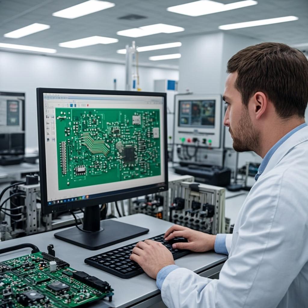
Adoption of advanced technology and manufacturing equipment Perfect production system Fast turnaround

Good quality control

Mature ISO9001/IATF16949 quality management system. Perfect ERP and MaS order management system.

Affordable price

Professional cost control engineers Cooperation with many raw material companies.

Professional engineering

Free DFM inspection of PCB files and BOMs. PCB engineering evaluation and advice.

Wide range of services

Specialized in medical, automotive, consumer electronics, new energy pcb. Serving global enterprises

The introduction and advantage of high frequency PCB

High-frequency PCB board refers to a printed circuit board above 1GHz. This definition may be different in the industry. Its physical performance, accuracy, and technical parameters are very high. They are often used in the fields of communication systems, car ADAS systems, satellite communication systems, and radio systems.

The characteristics of high-frequency PCB

High-frequency PCB is a circuit board for high -frequency signal transmission. It has the following characteristics:

  1. Low loss: High-frequency PCB uses better materials and special process design, which can reduce the loss of signals during transmission and maintain lower signal attenuation.
  2. Low noise: Special design and shielding technology adopted by high-frequency PCB can reduce the generation and dissemination of noise, and provide clean signal output.
  3. Good impedance matching: High -frequency PCB can achieve effective impedance matching with other high-frequency devices through accurate design and debugging to improve the efficiency of signal transmission.
  4. Strong anti-interference ability: High-frequency PCB has good anti-interference ability, can work normally in a complex electromagnetic environment, and reduce the impact of external interference on signals.
  5. The dielectric constant is small and stable: Generally speaking, the smaller the dielectric constant, the better because the square root of the signal transmission rate is the opposite of the square root of the material of the material. At the same time, the medium consumption requirements are small because this will mainly affect the quality of signal transmission.
  6. Thermal expansion coefficient is consistent with copper foil: If the thermal expansion coefficient is not synchronized, it will cause copper foil to be separated during hot and cold.
  7. Excellent heat resistance, chemical resistance, impact strength and separation strength: These characteristics ensure the stability and reliability of high-frequency PCB in harsh environments.

Application of High frequency PCB

Satellite communications

Wearable device

Medical diagnostic equipment

Industrial equipment

Our Manufacturing Capabilities

We manufacture high-frequency PCBs with frequency typically in the range from 500MHz to 2GHz.

FeatureCapability
Quality GradeStandard IPC 2
Number of Layers2 – 42layers
Order Quantity1pc – 10000+pcs
Build Time2days – 5weeks
MaterialRO4003C, RO4350B, Ro3003, Ro3010, RT5880
PPRogers 4450F, Domestic-(25FR), Domestic-(RF-27), Domestic-(6700)
Board SizeMin 6mm x 6mm | Max 457mm x 610mm
Board Thickness0.4mm – 5.0mm
Copper Weight(Finished)0.5oz – 2.oz
Min Tracing/Spacing3mil/3mil
Solder Mask SidesAs per the file
Solder Mask ColorGreen, White, Blue, Black, Red, Yellow
Silkscreen SidesAs per the file
Silkscreen ColorWhite, Black, Yellow
Surface FinishElectroless nickel/immersion gold (ENIG) – RoHS Immersion silver – RoHS Immersion tin – RoHS Organic solderability preservatives – RoHS
Min Annular Ring4mil
Min Drilling Hole Diameter6mil
Impedance tolerance±10%
Other TechniquesPeelable solder mask Gold fingers Carbon oil Countersink holes

Case Products

Solar controller motherboard

MRI Control Motherboard

Fire Alarm System Control Panel Replacement Board

Get a free quote,Please give me your requirements

Name *

E-Mail *

Phone number*

Message

CONTACT INFO

Address:4th–6th Floors, Xingyuan Technology Park, Tongda Road, Gushu, Xixiang Town, Bao’an District, Shenzhen, Guangdong Province, China

Factory:A3 区Area A3, Phung Nenh Truce Industrial Zone (Nam Giang Industrial Park), Viet Yen City, Bac Giang Province, Vietnam

WhatsApp:+86 15919758327

Tel: +86-15919758327

Tel : +86-755-23108895

Fax : +86-755-29129721

Contact : Victor Zhang

Email :pcb@frankenthalerfoundation.org

LATEST PRODUCTS
  • Smart video doorbell PCB module developed based on ESP32-s3 chip 09/10/2025 - 02:53
  • ESP32 Smart Medicine Cabinet Development Solution 09/04/2025 - 02:33
  • Banana Pi BPI-M5 Pro open source single board computer pcb module 06/13/2025 - 03:04
BLOG
  • Deep Analysis of PCB Copper Cladding vs. Copper Pouring: 5 Key Differences 03/11/2026 - 07:03
  • Complete Guide to PCB Co-design in 2026 03/09/2026 - 03:29
  • Custom PCB vs. Standard PCB: The Ultimate Selection Guide and Key Differences Explained