01/
Cost Reduction
This is the most important benefit of your long term relationship with us. After learning your specific needs, we will quickly work out a tailored integrated solution to meet your expenses and cost reduction targets.
02/
Certified Quality Standards
Our quality assurance policy is not based on company integrity alone. It is also affirmed by various certifications recognized across North America. We are known for delivering only the best, most durable assemblies.
03/
Create Value for the Customer
We work with our customers on an individual basis, making sure what we deliver matches your needs precisely. Moreover, we have a staff of Program Managers on board that help clients work out those needs, helping develop a raw idea into a comprehensive PCB Fabrication or PCB Assembly.
04/
Flexibility
We react quickly to your changing needs. Our working time and style is flexible to meet your variable needs. To us, your requirements are our guidelines and rules to follow.
High Frequency PCB is a form of PCB where the printed circuit boards have higher electromagnetic frequency, often used in applications that require the transfer of specific signals between two objects. It can operate between 500 MHz and 2 GHz, making it an excellent choice for mobile, microwave, RF, and other high-speed design applications. A frequency above 1GHz is considered high frequency.
PCB Rogers 4350b
Rogers RO4350B is a hydrocarbon/ceramic laminate with a dielectric constant of 3.48. It meets the
Rf PCB Rogers 4003
RO4003C is a patented hydrocarbon resin system/ceramic filler material reinforced with woven glass
Rogers PCB(RO4003C, RO4350B, RT5880)
Rogers RO3003 high frequency circuit material is a PTFE composite material with ceramic filler. The
Rogers + FR4 Mixed Delectrics PCB
Material: Rogers RO4350B+FR4. Layer Number: 4 Layer. Board thickness: 1.2mm.
Make a PCB Design
Begin by laying out the PCB blueprint on your preferred design software. You can use Extended Gerber to encode the blueprint, then send the file to the fabricator for manufacturing.
Print the PCB Design
Also, print the PCB design, and you can use a plotter printer to produce a PCB film, which is a negative for the blueprint. It has two inks: black shows the conductive copper lines, while clear ink indicates the non-conductive sections.
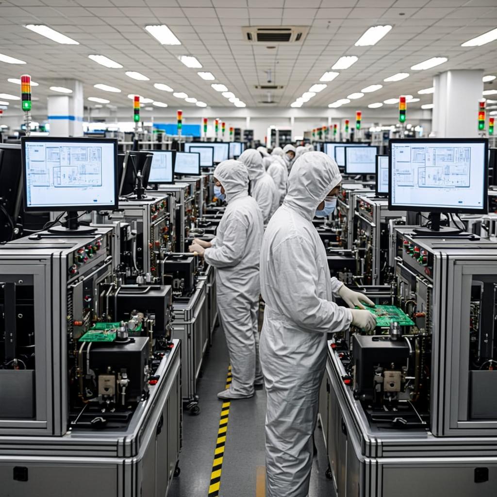
Print Copper for the Inner Layers
Manufacturing begins at this stage, and after printing the PCB on the laminate, copper gets pre-bonded on the same laminate, which acts as the PCB structure. Next, engrave the copper to reveal the initial blueprint.
Alignment of Layers
Since a high-frequency PCB has different layers, manufacturers usually use optical punches to align them by forcing pins down the holes. Another machine checks whether the layers are in order and without defects.
PCB Layers Lamination
The next stage involves fusing or laminating the layers and layup steps if there are no defects. Prepare the inner and outer sections, then use a metal clamp to help join them.
Drilling
Use a computer-guided drill with the guidance of the Extended Gerber design to do the drilling. But before that, use an X-ray machine to determine the drilling spots. After drilling, file off the excess copper to leave the surface smooth.
Plating of PCB
Plating involves joining the layers together using chemicals. But first, you must clean the boards thoroughly before dipping them in the chemicals.
Solder Masking
Next, clean the panels again before applying the solder mask, then use epoxy ink with the solder film. Expose the board to UV light to remove the solder mask parts.
Screening and Finishing of Silk
As described earlier, the finishing process involves plating the board with gold, silver, or HASL to prevent oxidation. Afterward, silkscreen the PCB to print all the essential details, such as the manufacturer name and warning labels.
Testing
This process checks the circuit isolation and continuity to ensure no shorts or disconnections exist.
Cutting
The last step is cutting the PCB using a CNC machine or a V-a groove.
PCB Rogers 4350B
Signal Integrity
High-frequency signals are susceptible to various forms of interference and degradation. Proper PCB design minimizes signal losses, reflections, and electromagnetic interference (EMI), ensuring reliable signal transmission.
Impedance Matching
Impedance matching is crucial in high-frequency circuits to prevent signal reflections. A well-designed PCB maintains consistent impedance across traces and components.
Minimized Crosstalk
Crosstalk between traces can lead to signal distortion. Careful design techniques help minimize Crosstalk, preserving signal quality.
EMI/EMC Compliance
High-frequency devices must adhere to electromagnetic interference (EMI) and electromagnetic compatibility (EMC) regulations. Correct PCB design aids in achieving compliance.
Heat Dissipation
High-frequency components generate heat. Effective thermal management is necessary to prevent overheating and ensure long-term reliability.
1
Material Selection:Choosing the right substrate material is crucial for high-frequency PCBs. Materials with a low dielectric constant (Dk) and low dissipation factor (Df) are preferred to minimize signal loss and maintain signal integrity. Common materials used for high-frequency PCBs include specialized laminates like Rogers, Teflon (PTFE), Arlon, and Isola.
2
Controlled Impedance:High-frequency signals require precise impedance control to minimize signal reflections and maintain signal integrity. PCB traces are designed with specific widths, thicknesses, and spacing to achieve the desired characteristic impedance. Controlled impedance helps prevent signal degradation and ensures reliable performance.
3
Transmission Line Structures:High-frequency PCBs often utilize transmission line structures, such as microstrip and stripline, to transmit signals effectively. Microstrip cons