flexible pcb
Automotive flexible pcb
Material: Rogers 5880
Layers: Four
Dielectric Loss Factor: 0.0037
Board Thickness: 0.8 + 0.1 mm
Minimum Line Width/Spacing: 0.35mm/0.2mm
Process Characteristics: Taconic high-frequency materials
Minimum Hole Diameter: 0.3mm
Surface Treatment: Immersion Gold
Rogers high-frequency PCBs, produced by Rogers Corporation in the USA, offer excellent high-frequency performance, thermal stability, and mechanical strength, making them widely used in wireless communication, microwave technology, and high-speed digital applications.
Substrate Material: Rogers high-frequency PCBs use ceramic or special polymer composite materials, such as amide resin, which possess low dielectric constant (DK) and low dielectric loss, resulting in more stable signal transmission and reduced signal loss and crosstalk.
Epoxy-Free: Rogers PCB materials do not contain epoxy resin, which helps maintain low dielectric constant and dielectric loss, as well as excellent temperature stability.
High-Frequency Performance: Rogers high-frequency PCBs excel in high-frequency applications, capable of transmitting signals at higher frequency ranges with reduced signal loss and crosstalk, suitable for high-speed digital circuits and microwave communication.
Low Dielectric Constant and Loss: The substrate of Rogers PCBs features a low dielectric constant and low dielectric loss, contributing to better signal integrity and lower transmission loss.
Thermal Stability: Rogers PCBs maintain good stability and reliability in high-temperature environments, with a low coefficient of thermal expansion (CTE) ensuring stable operation in high-temperature and high-humidity conditions.
Mechanical Strength: The materials used in Rogers PCBs are hard and durable, capable of withstanding significant mechanical loads, ensuring reliable operation in various complex working conditions.
High Precision and Stability: The board thickness control is highly precise, copper adhesion is strong, heat dissipation is excellent, and there is no delamination or bubbling, ensuring long-term stability and reliability of the PCB.
The production process of Rogers high-frequency PCBs includes high-precision cutting technology, surface treatment, copper foil coating, high-speed electroplating process for drilling, electrolytic copper plating for circuit layer fabrication, circuit pattern drawing, and rigorous final product testing. These processes ensure the high precision and reliability of Rogers PCBs.
Communication Technology: Used in high-frequency antennas, base station antennas, etc., the stable dielectric performance and excellent thermal stability of Rogers PCBs ensure efficient operation of communication equipment in complex environments.
Military and Aerospace: In critical equipment such as radar, satellites, and missiles, the high strength and high-temperature resistance of Rogers PCBs enable these devices to operate stably under extreme conditions.
Medical Equipment: Used in medical monitoring instruments, pacemakers, MRIs, etc., their high stability and reliability ensure the accuracy and safety of medical devices.
Automotive Electronics: In areas like in-car navigation, audio systems, and body control, the excellent mechanical strength and thermal stability of Rogers PCBs enhance the stability and comfort of automotive electronic systems.
Number of layers 1-48 layers
Materials FR4, Tg=159197583270210, cem-3, cem-1, aluminum substrate, PTFE, Rogers, Nelco
Copper thickness 1/2oz, 1oz, 2oz, 3oz, 4oz, 5oz
Board Thickness 8-236mil (0.2-6.0mm)
Minimum line width/spacing 3/3 million (75/75um)
Minute drilling size 8 million (0.2 mm)
Min HDI laser drill size 3 million (0.067 mm)
Aperture tolerance 2 million (0.05 mm)
PTH copper thickness 1 million (25 microns)
Resistance welding color Green, Blue, Yellow, White, Black, Red
Strippable solder mask layer yes
surface treatment HASL (ROHS), ENING, OSP, sinking silver, sinking tin, shining gold, golden fingers
Gold thickness 2-30u (0.05-0.76um)
Blind hole/buried hole yes
V-shaped cutting yes
No products found!
Layers: 2 layers
Board Thickness: 0.635mm ± 0.05mm
Substrate Material: 96% Silicon Nitride
Surface Finish: ENIG (Electroless Nickel Immersion Gold)
Thermal Conductivity of Insulating Layer: 85 W/m·K
Outer Copper Thickness: 200μm
Gold Thickness: ≥ 3μ
Process Characteristics: AMB process
Board Thickness: 0.5 mm
Base Material: Aluminum Oxide
Copper Thickness: 100 μm
Process Feature: DPC (Direct Plated Copper) Process
Surface Finish: ENIG / Silver (2μ)
Dimensions: 70 × 70 mm
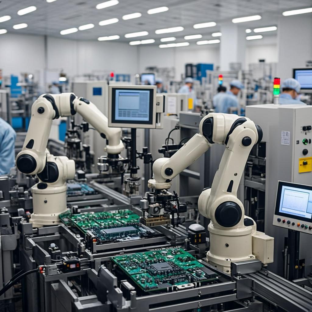
Number of SMT lines: 7 high-speed SMT mating lines
SMT daily production capacity: more than 50 million points
Inspection equipment: X-RAY tester, first piece tester, AOI automatic optical tester, ICT tester, BGA rework station
Mounting speed: CHIP component mounting speed (optimal conditions) 0.036S/chip
Minimum package: 0201, accuracy up to +0.04mm
Minimum device accuracy: PLCC, QFP, BGA, CSP and other devices can be pasted, with pin spacing up to +0.04mm
IC-type placement accuracy: the mounting of ultra-PCB boards, flexible PCB boards, gold fingers, etc. has a high level, can be mounted/inserted/mixed TFT display driver boards, cell phone motherboards, battery protection circuits and other difficult products.