Candor’s HDI PCBs are engineered for precision, performance, and compact designs. With advanced manufacturing techniques and state-of-the-art equipment, our HDI boards meet the demands of cutting-edge technology applications. Designed for reliability and efficiency, these boards optimize space, improve signal performance, and reduce cost without sacrificing quality. Perfect for industries requiring high-density components in minimal spaces. Contact us today for a quote tailored to your needs.
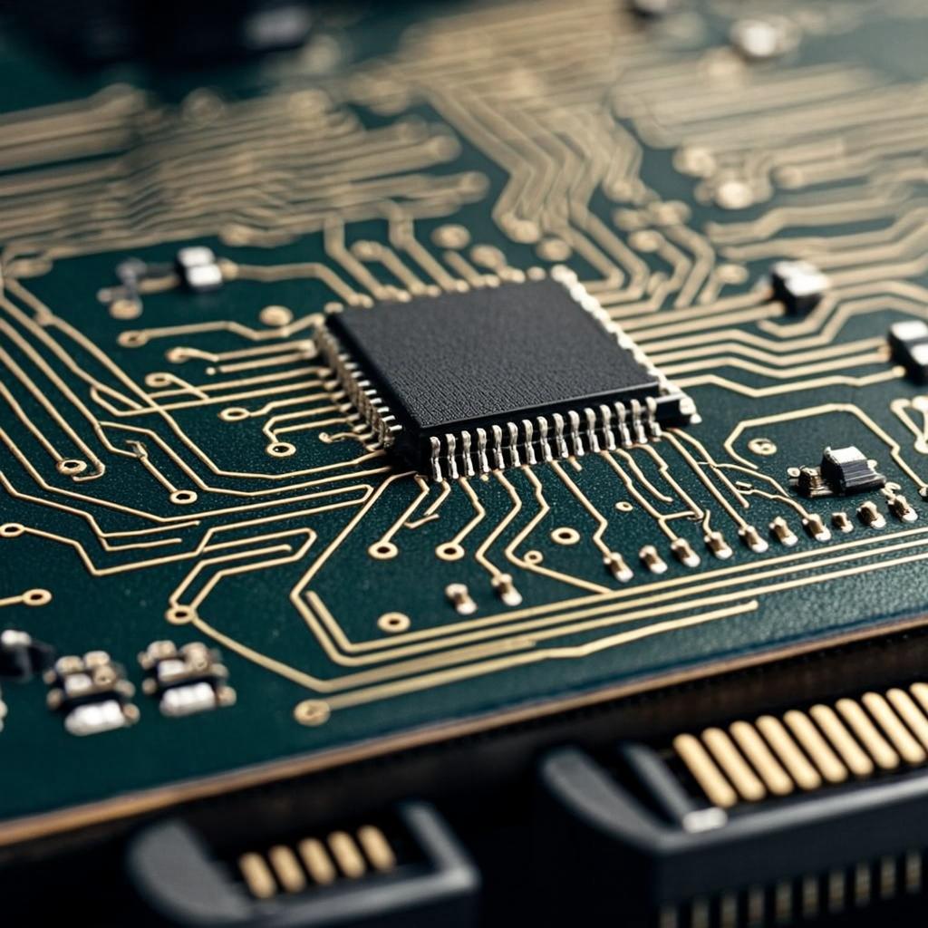
High-Density Interconnect (HDI) PCBs are advanced multi-layered circuit boards designed to deliver superior functionality in compact spaces. Unlike traditional PCBs, HDI boards feature densely packed wiring and pad connections on high-density substrates. This technology enables smaller, lighter boards with enhanced electrical performance, making them essential for modern, complex electronic systems.
Candor’s HDI PCBs are crafted to reduce size and weight, making them ideal for compact devices. These designs enable multi-functional systems to fit seamlessly into space-constrained applications without sacrificing performance.
With advanced technology, our HDI PCBs ensure faster signal transmission and enhanced impedance control. Reduced crosstalk and interference guarantee high accuracy and reliability for critical applications.
Candor’s precision engineering allows for smaller vias and capture pads, enabling tighter spacing and higher pad density. This supports more components in less space, perfect for high-density circuitry.
Induction lamination strengthens multi-layer boards with superior bonding and heat distribution. Paired with epoxy filling, it ensures reliable connections and reduces the risk of delamination or failure.
Our compact and efficient designs reduce material usage and streamline production processes. Simplified drilling and fewer layers lower production time and costs, delivering value without compromising quality.
Candor’s HDI PCBs are designed to meet the demands of emerging technologies such as IoT, AI, and 5G. These versatile boards are ready to power the next generation of smarter, more advanced devices.
Ideal for advanced driver assistance systems (ADAS) and infotainment, HDI PCBs enhance vehicle safety, performance, and connectivity.
Compact and durable, HDI PCBs handle high-performance requirements for navigation, communication, and mission-critical systems.
Essential for 5G and high-frequency applications, HDI PCBs ensure fast signal transmission and reliable connectivity for global networks.
HDI PCBs improve performance in robotics, sensors, and control systems, supporting the efficiency of automated industrial processes.
HDI PCBs power compact devices like smartphones, tablets, and wearables, enabling high functionality in small form factors for modern consumers.
HDI PCBs feature a method of layer accumulation that starts with a traditional dual-sided board that is then laminated with layers. Compared to conventional circuit boards, these PCBs are lighter, thinner, and shorter, providing several advantages. Unlike ordinary PCBs, HDIs are made with micro-blind and / or buried vias. These are prepared using lasers, enabling an increase in the number of layers and aspect ratio compared to traditional PCBs.
The density of holes, lines, and pads in HDIs makes them particularly important for high-density plates and packing substrates that require precise impedance matching versus traditional boards.
HDI PCBs enable more compact end-product layers, as well as delivering improved standards of electrical performance and efficiency. With their higher interconnect density, improved signal strength, and increased reliability, HDI boards provide better protection against static discharge and thermal conduction. This enables these boards to handle load capacities that are impossible for traditional PCBs.
In HDI boards, blind vias, micro vias, and buried vias are used to reduce the thickness of the board, accommodating more wiring density across the layers.
When a board has an improper stack-up build, this can result in poor performance, EMI issues, crosstalk, and vulnerabilities. Stack-up has to be built so that all the high-speed signals facilitate a signal return path.
The nature of HDI PCBs is more complex than that of traditional boards, differentiating them from pre-existing market PCBs. Overlooking any fault in their designs will result in an HDI PCB that fails to work as intended, reducing performance. HDI PCBs need to go beyond the regular production techniques of traditional circuit boards, mostly because of their components. This results in a more expensive board.
Complex PCBs have many layers. When the layer count is higher, it adds to the cost of production. Producing HDI PCBs isn’t a simple process, and with the added layers, it can make these circuit boards more of an investment.
The core of PCBs is their materials, and HDI circuit boards cannot survive with affordable or accessible materials. Rare materials can increase the cost, as they are hard to acquire and import.
PCB production is an extensive process. Many different steps go into circuit board production, including lamination and drilling. These individual steps can increase cost, and HDI boards require additional manufacturing techniques to ensure their quality and performance.
High-quality production requires smart design. Bulk production typically lowers costs, as producing HDI PCBs on a small scale can be quite expensive. Premium testing