If you're new to the world of printed circuit boards and wondering, "What is HDI PCB?" or looking for a clear guide on HDI PCB basics, you're in the right place. HDI stands for High-Density Interconnect, a type of PCB designed to pack more components into a smaller space using advanced manufacturing techniques like microvias and fine lines. This technology is essential for modern electronics, from smartphones to medical devices, where size and performance matter. In this beginner's guide, we'll dive deep into HDI PCB basics, explain what makes these boards unique, and provide a step-by-step understanding to help you grasp this cutting-edge technology.
High-Density Interconnect (HDI) PCB is a specialized type of printed circuit board that allows for a higher number of components to be placed in a smaller area. Unlike traditional PCBs, which rely on larger through-holes and wider traces, HDI boards use thinner lines (often less than 75 micrometers) and tiny microvias (holes smaller than 150 micrometers in diameter) to create dense, compact layouts. This results in lighter, smaller, and more efficient electronic devices.
Think of HDI PCBs as the backbone of modern gadgets. They're used in devices where space is limited, but performance can't be compromised—like in smartphones, tablets, and wearable tech. By enabling more connections per square inch, HDI technology supports faster signal transmission and better power efficiency, often achieving signal speeds up to 10 Gbps in high-end applications.
As technology advances, the demand for smaller, faster, and more powerful devices continues to grow. HDI PCBs are at the heart of this evolution for several reasons:
Statistics show that over 49% of electronic devices today rely on HDI technology, a significant shift from traditional designs, as the push for miniaturization continues to dominate the industry.
To fully understand HDI PCB basics, let's break down the unique features that distinguish these boards from standard PCBs:
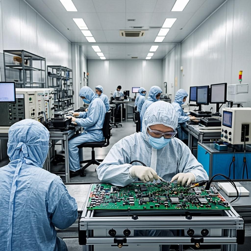
The manufacturing process for HDI PCBs is more complex than for standard boards due to the precision required. Here's a beginner-friendly look at the key steps:
This process requires advanced equipment and expertise, which is why partnering with a reliable PCB manufacturer is crucial for quality results.
HDI PCBs are a game-changer in industries where compact, high-performance electronics are essential. Here are some common applications:
Understanding the pros and cons of HDI PCBs can help you decide if they're the right choice for your project. Let's explore both sides:
If you're new to HDI PCB design, here are some practical tips to help you navigate the process:
As electronics continue to evolve, HDI PCB technology is also advancing. Here are a few trends to watch:
High-Density Interconnect (HDI) PCBs are revolutionizing the way we design and build electronics. By allowing more components to fit into smaller spaces with improved performance, they’re enabling the next generation of compact, high-speed devices. Whether you're an engineer just starting out or a hobbyist curious about advanced PCB technology, understanding HDI PCB basics is a valuable step toward mastering modern electronics.
This HDI PCB guide for beginners has covered the essentials—from what HDI PCBs are and how they’re made to their applications and design challenges. With this foundation, you’re better equipped to explore the world of high-density interconnect technology and apply it to your projects. Remember, partnering with a reliable PCB manufacturer can make all the difference in turning your HDI designs into reality.