1. What Makes High-Density PCBs the Most Difficult to Reverse Engineer
2. HDI Technology Features and Their RE Challenges
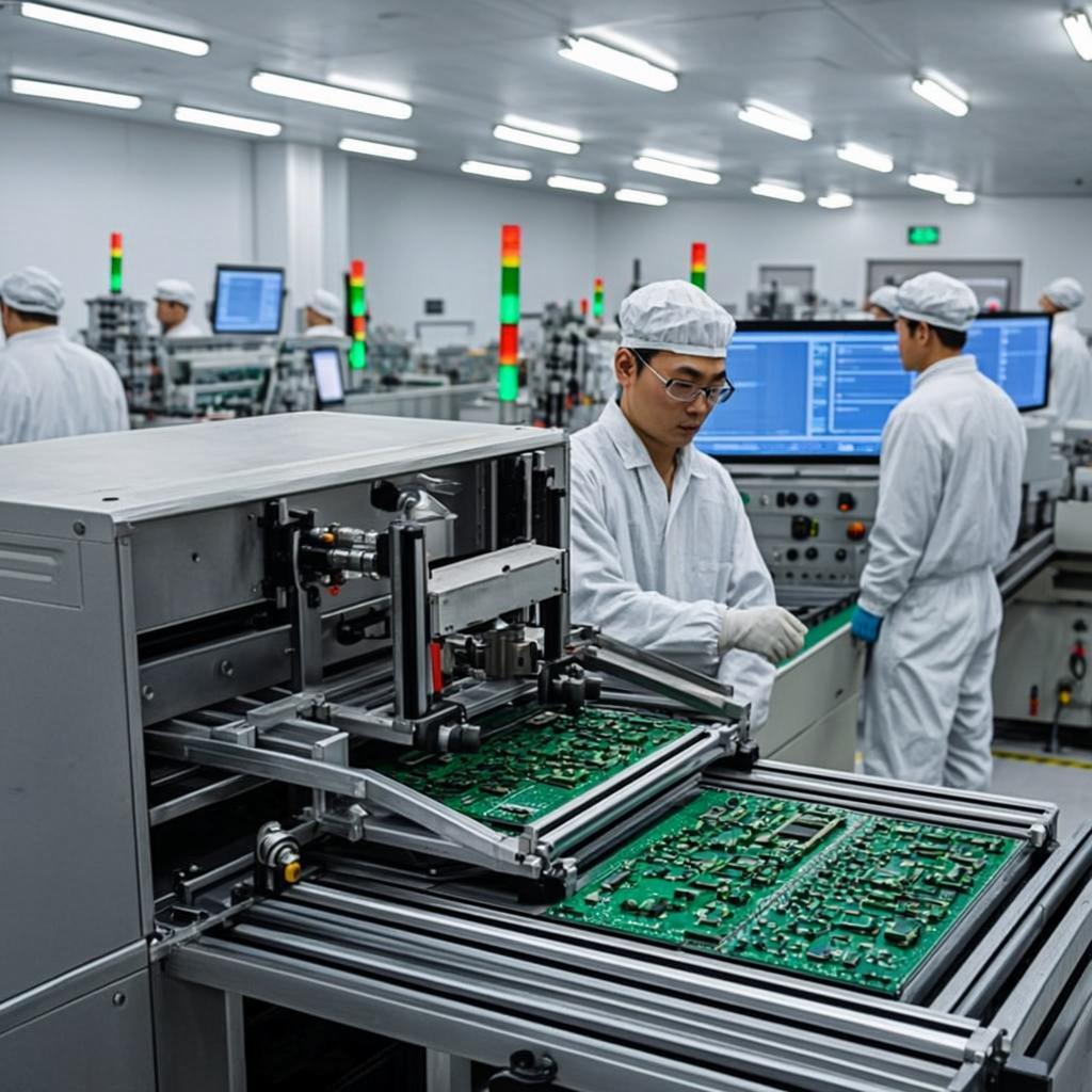
3. Imaging and Capture Methods for HDI Boards
4. Reconstructing HDI Layouts: Microvias, Sequential Lamination, and Stackup
5. BGA Component Analysis and Reconstruction
6. Verification and Manufacturing of HDI Replacement Boards
7. Highleap’s HDI PCB Reverse Engineering Services and IP Compliance
High density PCB reverse engineering tackles the most technically demanding boards in the electronics industry: multilayer HDI (High Density Interconnect) boards with microvias, blind and buried vias, fine-pitch BGA components at 0.4 mm or 0.3 mm ball pitch, trace widths below 75 µm, and layer counts of 10–20+. These boards are found in networking equipment, medical imaging devices, aerospace avionics, industrial control systems, and defense electronics — mission-critical platforms where replacement boards must be available long after the original manufacturer has discontinued production.
When critical HDI boards reach end-of-life and OEM support is no longer available, organizations face a choice: retire the entire system or reconstruct the board from physical analysis. PCB reverse engineering provides a legitimate path to manufacturing replacement boards for legacy system sustainment, obsolescence management, failure analysis, and second-source qualification — all within intellectual property laws and contractual obligations.
The reverse engineering challenge scales dramatically with board density. A standard 4-layer board with 0.2 mm traces and 0.8 mm-pitch QFP components can be reverse engineered with optical scanning and basic X-ray. An HDI board with 0.05 mm traces, 0.075 mm microvias, and 0.3 mm-pitch BGA requires CT scanning, specialized imaging software, and engineers experienced with advanced fabrication processes. The margin for error shrinks proportionally — a 0.025 mm positioning error on a standard board is invisible, but on an HDI board with 0.1 mm trace-to-trace spacing, the same error creates a short circuit.
This guide covers the specialized methodology for reverse engineering HDI PCBs, from the imaging technology required through microvia reconstruction to manufacturing validation.
HDI boards use sequential lamination — they are built up in stages, with microvias laser-drilled at each stage, rather than being drilled and plated in a single pass like standard boards. This creates via structures that connect specific layer pairs (Layer 1–2, Layer 2–3) rather than penetrating the entire board. The reverse engineer must determine not just where each via is, but which specific layers it connects — a determination that requires CT scanning or destructive cross-sectioning.
Microvias (≤0.15 mm drill diameter) are the defining feature of HDI PCBs. They are laser-drilled (not mechanically drilled) and connect adjacent layer pairs. Types include:
Fine-pitch BGA components require via-in-pad technology — vias placed directly in the component pad rather than offset to the side. These vias are typically filled with copper or epoxy and plated over to create a flat pad surface for BGA soldering. The reverse engineer must identify via-in-pad structures (often invisible from the surface after filling and plating) to correctly map layer connectivity under BGA components.
Some HDI boards embed passive components (thin-film resistors, capacitors) within the board substrate. These components are invisible from the surface and can only be detected by electrical measurement (unexpected resistance or capacitance between points that appear directly connected on the surface) or high-resolution CT scanning.
CT (computed tomography) scanning is effectively mandatory for HDI reverse engineering. Standard 2D X-ray cannot resolve individual layers on a 12-layer board with microvias — all layers are superimposed in the image. CT creates a full 3D volume that can be “sliced” at each layer depth, revealing:
Resolution requirements: CT scans for HDI boards need voxel sizes of 5–15 µm to resolve 0.050–0.075 mm traces. This limits the maximum board area that can be scanned in one pass — large boards may require multiple overlapping scans that are stitched together.
After component removal, outer layers are captured at high resolution using digital microscope cameras (5–10 µm per pixel). The imaging system must handle:
For stackup verification: microsection analysis at multiple locations across the board to measure:
The stackup of an HDI board is significantly more complex than a standard board:
Accurate stackup reconstruction is critical for impedance calculations. HDI boards commonly have controlled-impedance traces (50Ω single-ended, 100Ω differential) on multiple layers — incorrect dielectric thickness in the stackup specification will produce incorrect impedance.
Using CT scan data, every microvia is mapped:
For a complex HDI board, the microvia count may reach several thousand — each requiring correct layer assignment. This is the most time-consuming aspect of HDI reverse engineering.
The BGA fanout — the trace routing pattern that connects BGA pads to vias and outward to the board’s signal routing layers — is the most geometrically constrained area on an HDI board. At 0.4 mm BGA pitch, traces must route between pads with 0.100 mm spacing — leaving approximately 0.050 mm trace width with 0.025 mm clearance on each side. These dimensions must be captured with corresponding accuracy.
BGA components have their connections on the bottom surface, invisible when the component is installed. The ball map (which balls are connected and which are no-connect) must be determined from:
BGA footprints require the highest positional accuracy in the reconstruction:
The reconstructed HDI layout must pass DRC against the target manufacturer’s HDI capability profile:
For controlled-impedance HDI boards, the reconstructed stackup and trace dimensions must produce the correct impedance. This is verified by:
HDI boards require specialized manufacturing capability — not every PCB fabricator can produce them:
Fabrication facility selection must match the board’s technology requirements — attempting to manufacture an HDI design at a standard-capability shop will result in fabrication failures and quality problems.
Our commitment to lawful practice: Highleap provides PCB reverse engineering exclusively for legitimate purposes including legacy system sustainment, end-of-life component replacement, failure analysis, second-source qualification, and interoperability development. Every project is evaluated for IP compliance before acceptance. We do not accept projects intended to replicate proprietary products for market competition or circumvent active patent protections. Clients are required to confirm lawful ownership or authorization of the boards submitted for analysis.
Highleap Electronics provides specialized HDI reverse engineering with the imaging technology, engineering expertise, and manufacturing capability required for high-density boards: