Helen Frankenthaler PCB Circuit Board R&D Center

High Speed PCB Mass Production PCB Assembly

PCB Assembly Manufacturing Process Flow Chart 2025

Introduction

In 2025, as electronics grow increasingly compact and complex, the PCB assembly (PCBA) process becomes more critical than ever. The accuracy, efficiency, and quality of this process directly impact product performance, reliability, and time to market. This article details the full PCB assembly manufacturing process flow chart for 2025 with insights into each step and how trusted partners like Wintech deliver superior outcomes.

Why PCB Assembly Is Critical

PCB assembly bridges the gap between design and reality. Without precise PCBA processes, even the most advanced electronic designs would fail due to:

  • Poor signal integrity
  • Component misalignment or defects
  • Electromagnetic interference (EMI)
  • Low mechanical durability
  • Functional inconsistency

Overview of the PCB Assembly Process Flow

Below is a step-by-step breakdown of a modern PCB assembly process in 2025. The flow includes both surface-mount technology (SMT) and through-hole technology (THT), applicable to both low and high-volume production environments.

Step 1: PCB Design & Layout

The foundation of a successful assembly process begins with a precise PCB layout. At Wintech, we offer high-level, high-difficulty, and large-size PCB layout services using industry-leading CAD tools.

  • Design rule checks (DRC)
  • Signal and power integrity analysis
  • High-speed design support
  • Thermal management planning

Step 2: PCB Fabrication

Wintech’s in-house fabrication includes multilayer PCBs with high-precision tolerances. This step involves:

  • Inner layer imaging and etching
  • Lamination and drilling
  • Plating through-holes and vias
  • Solder mask and silkscreen application

Step 3: Component Procurement

Sourcing reliable and authentic components is crucial. Wintech manages BOM validation, vendor sourcing, and inventory tracking with a global network of suppliers.

  • Quality-approved suppliers
  • Counterfeit component screening
  • Short lead time procurement

Step 4: Solder Paste Printing

Solder paste is applied to SMT pads using stainless-steel stencils. Key aspects include:

  • Controlled temperature and humidity
  • Stencil alignment and aperture size control
  • Paste thickness verification

Step 5: Pick and Place

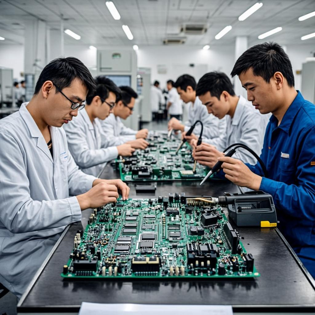
Automated pick-and-place machines position components with sub-millimeter accuracy. This step is tailored to both high-mix, low-volume and mass production projects at Wintech.

  • Vision-guided alignment
  • Placement rate: up to 80,000 CPH
  • 0402 to BGA package support

Step 6: Reflow Soldering

The board passes through a reflow oven where solder paste melts and solidifies, bonding components. Wintech uses lead-free, RoHS-compliant processes with profile tuning.

  • 12-zone reflow ovens
  • Profile optimization for each assembly
  • Temperature-controlled solder joints

Step 7: Inspection and Quality Control

Post-reflow, boards are inspected to detect misaligned or defective components using:

  • AOI (Automated Optical Inspection)
  • X-ray Inspection for BGA and QFN packages
  • SPI (Solder Paste Inspection)

Step 8: Through-Hole Component Insertion

For PCBs with THT components, parts are manually or robotically inserted. At Wintech, experienced technicians handle this process for precision and speed.

Step 9: Wave Soldering

In THT assemblies, the board is passed over a wave of molten solder to fix components on the opposite side.

  • Consistent solder joints for large-scale assemblies
  • Flux application and preheating included

Step 10: Final Assembly & Box Build

PCBs are integrated into enclosures or subassemblies. Wintech’s turnkey box build solutions include:

  • Enclosure installation
  • Wiring and cable harnessing
  • Labeling, packaging, and documentation

Step 11: Functional Testing

Functional testing verifies real-world performance. Depending on the complexity, we conduct:

  • ICT (In-Circuit Test)
  • Boundary scan
  • Burn-in and stress testing

Step 12: Packing & Delivery

After passing QA, products are securely packed for global shipping. Wintech offers:

  • Anti-static and ESD-safe packaging
  • Custom foam inserts and labeling
  • Fast, tracked international delivery

Why Choose Wintech for PCB Assembly?

Wintech is a trusted electronics manufacturing service (EMS) provider specializing in high-mix, low-to-mid volume projects with custom material integration. We offer:

  • Complete turnkey solutions from design to box build
  • Expertise in large, high-precision, and complex PCBs
  • Dedicated to quality, speed, and customer satisfaction
  • Partnerships with many of the world’s top 500 enterprises

Conclusion

The PCB assembly process in 2025 requires precision, technology, and experience. From the initial design to final testing and packaging, every step must be controlled and optimized. With a full turnkey model, Wintech leads the way in offering custom, scalable, and high-quality PCBA solutions for global clients.

Summary Table

StepDescriptionTechnology Used
1. PCB LayoutDesigning circuitry and layersCAD tools, simulation, DRC
2. PCB FabricationManufacturing bare PCBEtching, lamination, drilling
3. Component ProcurementSourcing and verifying partsBOM management, vendor screening
4. Solder Paste PrintingApplying paste to padsStencil printer
5. Pick and PlaceMounting SMT componentsAutomated placement machine
6. Reflow SolderingBonding components via heatReflow oven
7. InspectionChecking assembly accuracyAOI, X-ray, SPI
8. THT InsertionAdding through-hole componentsManual or robotic insertion
9. Wave SolderingFixing THT with molten solderSolder wave machine
10. Box BuildAssembly into final productWiring, enclosure, packaging
11. Functional TestingPerformance verificationICT, boundary scan
12. Packing & ShippingPreparing for deliveryESD-safe packaging, labeling