Whether rigid or flexible, high-frequency PCBs enable faster signal transmission rates and support operating frequencies up to 100 GHz. Their performance is enhanced by materials specifically selected for their low dielectric constant (Dk), low dissipation factor (Df), and minimal thermal expansion. HF PCBs are commonly used in high-density interconnect (HDI) technology and are essential components in high-speed communications, telecommunications, and radio frequency (RF) microwave applications.
Fastlink is a China-based professional PCB manufacturer that offers reliable and high-performance high-frequency PCB fabrication services. We can produce high-frequency PCBs typically in the range of 500MHz to 10GHz.
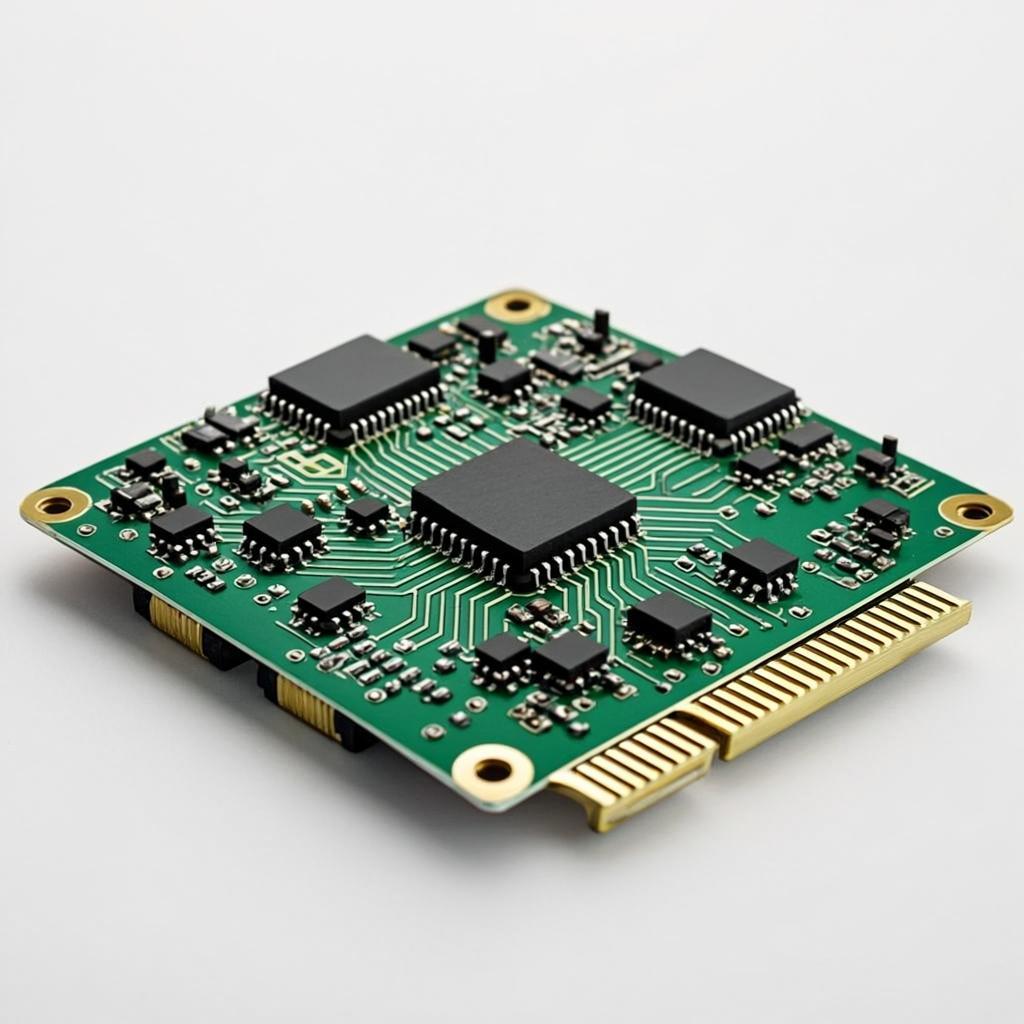
High-frequency PCBs work by using specialized materials and design techniques to handle signals that operate at high frequencies, which are typically above 1 GHz. These signals require smooth copper surfaces, low dielectric constant materials, and tight control of impedance to minimize signal losses and distortion. The PCB’s substrate is often made from materials like PTFE (Teflon) or advanced resin to maintain signal integrity. The design may include microstrip or stripline configurations to manage the path of the signals, and the layout is optimized to prevent crosstalk and electromagnetic interference, which are critical at high frequencies.
The Rogers RO4000 series has been an industry leader. As a low-loss material, it’s frequently used in microwave and millimeter-wave frequency designs. Its ease of use in circuit production and consistent performance offer advantages over conventional PTFE materials.
Specifically, Rogers 4350B exhibits low loss and is suitable for applications in the 500MHz to 3GHz frequency range. Panasonic Megtron 6 is another low-loss material that is designed for the higher frequency range of 3GHz and above. Materials such as Isola I-speed, Isola Astra, and Tachyon exhibit excellent low-loss characteristics at high frequencies.
The fabrication of a high-frequency PCB begins with finalizing the board stack-up, which is the arrangement of various layers to ensure optimal performance. This critical step determines the dielectric properties and signal integrity. Once the stack-up is confirmed, layout design commences, routing signal tracks via specialized software, creating a blueprint that guides the subsequent fabrication steps.
Digital designs are transformed into physical films using a plotter printer, which prints the conductive and non-conductive areas with different inks. This stage is vital for accuracy in the etching process, as it delineates where copper should be preserved or removed.
The inner copper layers are prepared by first cleaning the copper-clad laminates to eliminate contaminants. These laminates, coated with photoresist, are then exposed to UV light, which hardens the photoresist in the areas that will become the circuit traces, ensuring precision in the pattern that will form the electrical pathways.
The etching process selectively removes unwanted copper, leaving behind the circuit pattern. This is achieved by washing away unhardened photoresist and then etching the exposed copper with an alkaline solution. This step requires precise control to maintain the integrity of the desired circuitry.
Each layer undergoes Automated Optical Inspection (AOI) against the design files to detect and correct any errors. Precise drilling of registration holes aligns the multiple layers in preparation for lamination, highlighting the importance of dimensional accuracy.
The layers are bound together using heat and pressure to melt prepreg material, forming a solid board structure. The drilling of vias and holes follows, incorporating X-ray alignment for accuracy, which is particularly crucial for maintaining the conductive paths in high-frequency applications.
The outer layers undergo similar preparation as the inner layers. Electroplating follows, depositing a conductive material on the walls of the drilled holes and vias to establish a continuous electrical pathway critical for signal transmission.
A solder mask is applied to protect the copper traces and prevent electrical shorts. Silkscreen printing then adds labels and component information, providing a guide for assembly and usage.
The final step is a comprehensive testing phase that ensures the PCB’s functionality by checking for continuity and proper isolation. After successful testing, the PCB is cut into individual boards, ready for delivery to the customer.
High-frequency PCBs are commonly used in applications where high-speed signal transmission is required, such as telecommunications, radar, and defense systems. Because of their unique properties, they are able to maintain signal integrity and minimize signal loss, which is crucial for these applications.
In addition to these applications, HF PCBs are also used in a variety of other industries, including consumer electronics, industrial automation, and transportation.
Please accept cookies to access this content
High-frequency PCBs demand advanced design and manufacturing techniques beyond those used for standard boards. They require precise alignment, copper plating, and high-temperature soldering of high-frequency components. Designers must carefully consider the electrical performance requirements of high-frequency applications to create high-quality boards that meet performance standards.
Fastlink is a trusted high-frequency PCB manufacturer with over 15 years of experience. We typically stock common high-frequency PCB laminates such as Rogers PCB, but it is always best to contact us in advance to ensure that we have the specific HF material you need for your new project.
Our 65,000-square-foot state-of-the-art facility in Shenzhen houses the advanced equipment for manufacturing and assembling printed circuit boards. Fastlink leads the industry in quality and performance, whether you need standard fast PCBs or metal PCBs with tight tolerances.
There are more pictures of our factory’s equipment display in our company profile.
We are duly certified with the following accreditations:
Furthermore, all our products adhere to the IPC & ROHS Standards. It is our continuous endeavor to produce premium quality PCB products