Helen Frankenthaler PCB Circuit Board R&D Center

high speed printed circuit boards a tutorial

Customized Printed Circuit Assembly, High-Speed Electronic Board Assembly

Customized Printed Circuit Assembly, High-Speed Electronic Board Assembly

Basic Information

Place of Origin:CHINA
Brand Name:TYF
Certification:CE UL CB
Model Number:PCBA
Minimum Order Quantity:Negotiation
Price:Negotiable
Packaging Details:carton
Delivery Time:10 workdays
Payment Terms:L/C, D/A, D/P, T/T, Western Union, MoneyGram
Supply Ability:100000 PCS/MONTH

Detail Information

Brand:TYFCopper Thickness:0.3-3oz
Base Material:FR4, Aluminum, FPCSurface Finishing:HASL, OSP, Lead Free
Services:One-stop ServicesMax Board Size:760mm*600mm
Layer:1-26layersCertificate:ISO9001/IATF16949/ISO13485
Highlight:printed circuit assembly , electronic circuit board assembly

Product Description

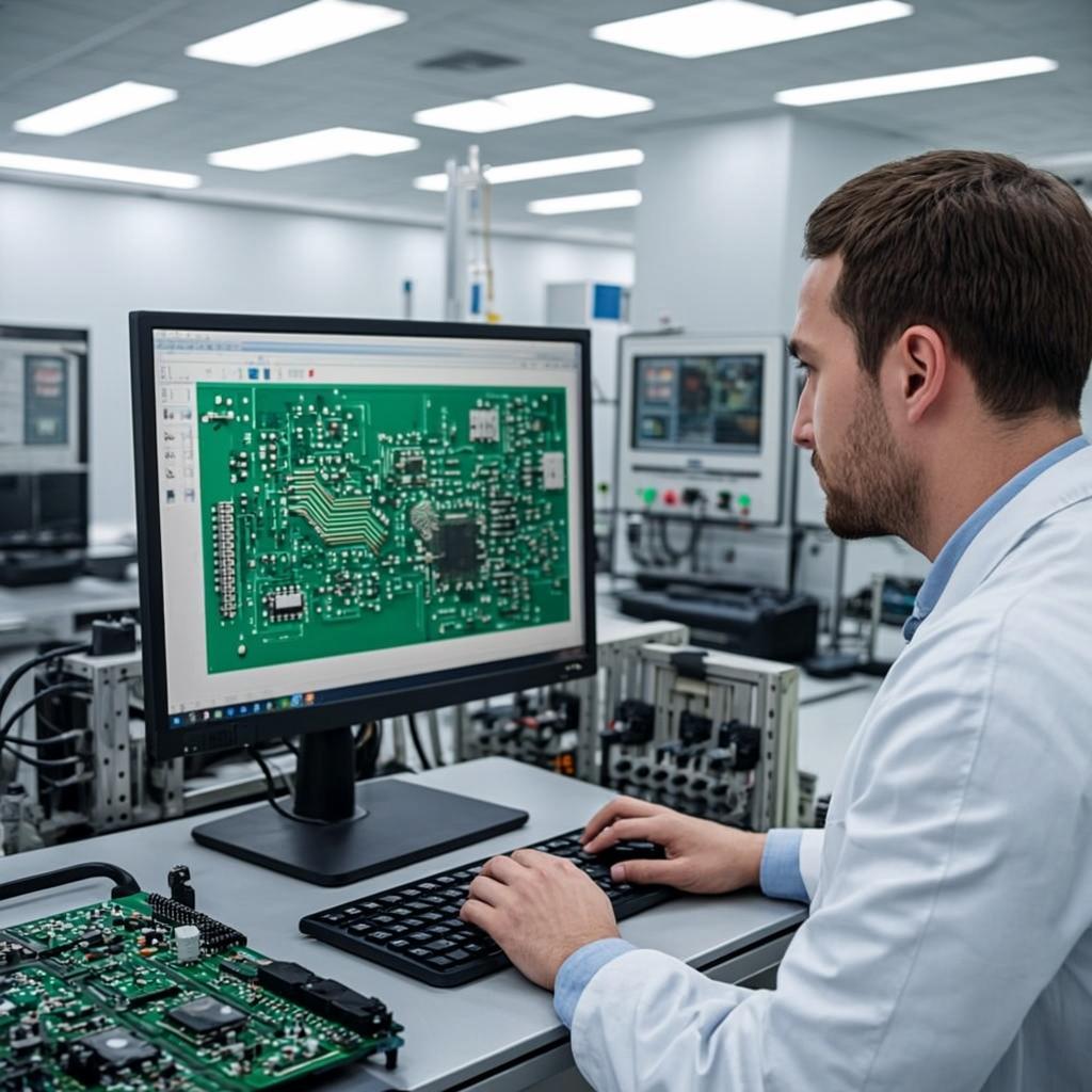
pcb board customized microcontroller development board, circuit board electronic pcb assembly

1. Details:

Item name: SMT Assembly PCBA PCBA

Place of Origin: ShenZhen, China

Model: TYF PCBA

MOQ: 1000 piece

2. PCB Design & Layout
  • Excellent Expertise in design tools: Allegro, Pads, and Mentor Expedition.
  • High density SMT designs (BGA, uBGA, PCI, PCIE, CPCI…)
  • Flex PCB designs of all sorts
  • Complete assembly drawings
  • In-Circuit Test data generation (ICT)
  • Drill, panel and cutout drawings designed
  • Professional fabrication documents created
  • High-speed, multi-layer digital PCB designs- Bus routing, differential pairs, matched lengths; Fast PCB design in 2-3 days.
  • Concentrate on the PCB design Wi-Fi Module, BLE Module, GPS Tracking application.RF Modules,Medical-Care devices,LED PCB Boards.
  • We come up with the design as per customer requirement,and take care for the RAW material cost at the outset of design.
  • Full control for the PCB design, from requirement, Schematic, PCB Layout, SI/PI/EMI inspection, we will locate the design issues in the inspection processing.
3. PCB Specifications

PCB layer 1, 2, 4 or 6, up to 18 layers

Board shape Rectangular, round, slots, cutouts, complex, irregular

Board type Rigid, flexible, rigid-flexible

Board material FR-4 glass epoxy, FR4 High Tg, RoHS compliant; Aluminum, Rogers, etc.

Board cutting Shear, V-score, tab-routed

Board thickness 0.2 ~ 4.0 mm (±10%), Flex board: 0.01 ~ 0.25″ (±10%)

Copper weight 1.0, 1.5, 2.0 Oz (tolerance ±0.25 oz)

Solder mask Double-sided green LPI, Also support red, white, yellow, blue, black

Silk screen Double-sided or single-sided in white,yellow, black, or negative

Silk screen min. line width 0.006″ or 0.15mm

Max board dimension 20 inch *20 inch or 500mm*500mm

Min. trace/gap 0.10mm, or 4 mils

Min. drill hole diameter 0.01”, 0.25mm, or 10 mils

Surface finish HASL, Nickle, Imm Gold, Imm Tin, Imm Silver, OSP etc.

Min.slot width 0.12”, 3.0 mm, or 120 mils

V-score depth 20-25% of board thickness

Plated through holes Yes

Design file format Gerber RS274X, 274D, Eagle and AutoCAD’s, DXF, DWG, Protel 99se

4. PCB Assembly Center

Supported Assembly Capabilities

Different types of Assembly
  • THD (Thru-Hole Device)
  • SMT (Surface-Mount Technology)
  • SMT & THD combined
  • 2-sided SMT and THD assembly
Order Volume Allowed

1 to 5,000 boards

Parts
  • Passives parts, smallest size 0201
  • Fine pitch to 8 Mils
  • BGA, uBGA, QFN, POP and Zero-Lead chips
  • Connectors and terminals
Component Package
  • Reels
  • Cut tape
  • Tube and tray
  • Loose parts and bulk
PCB Board Measurements

Minimum measurement: 0.2″ x 0.2″ (5mm x 5mm)

Largest dimension: 15″ x 20″ (381mm x 508mm)

Printed circuit board shapes
  • Oblong
  • Round
  • Slots and Cut outs
  • Complicated and Uncommon
PCB board kinds
  • Rigid FR-4 boards
  • Rigid-Flex boards
Assy procedures
  • Leaded process
  • ero-Lead (RoHS)
Design file formatting
  • Gerber RS-274X, 274D, Eagle as well as AutoCAD’s DXF, DWG
  • BOM (Bill of Materials) (.xls, .csv, . xlsx)
  • Centroid (Pick-N-Place Or XY file)
Testing Processes
  • Visual Inspection
  • X-ray Inspection
  • AOI (Also known as: Automated Optical Inspection)
  • ICT (AKA: In-Circuit Test)
  • Functional testing
Turnaround time periods

1 To 5 days for only printed circuit board assy

10 To16 days for full Turnkey Circuit Card Assy

5. Packaging

TYF Opto. LED modules products, packed in plastic Tray, according to different size, XX PCs each plastic Tray, as shown in the following. products without plastic box packed in bubble bags, in order to prevent the outside pressure, choose different bubble bag, according to the product size in each pack of XX products, packaged product will be stored in the form of carton and sealed, as shown in the following.

1) xx PCS LED module per Tray 4) Box information & packing

2)Tray stack and taping, XX LED module

trays and additional 1 dummy trays each up of

box. Add silica gel (1 each) on top of the tray

3) Sealing packing