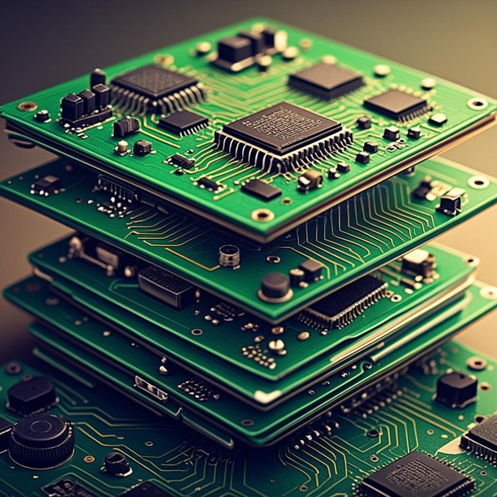
As the electronics industry continues to evolve, high-speed and high-frequency electronic products are rapidly emerging to meet the growing demands of the market. Against this backdrop, the design of high-frequency PCBs has become more critical than ever. Fields such as telecommunications, aerospace, medical devices, and high-performance computing are increasingly reliant on fast data transmission capabilities. To ensure signal integrity and system reliability, designers must adhere to a set of essential principles. This article explores the fundamental guidelines that engineers must follow when developing high-frequency PCBs to achieve optimal performance.
High-frequency PCB design focuses on creating circuit boards capable of accurately transmitting high-frequency signals. Before diving into the design process, it’s important to understand what constitutes high frequency and the specific rules that govern such designs. Adhering to these principles helps prevent signal distortion. Generally, frequencies above 1 GHz are considered high frequency, and conventional design techniques often fall short in meeting the demands of signal integrity and performance at this level. At such frequencies, interference can lead to signal attenuation, crosstalk, and electromagnetic interference (EMI).
In today’s fast-paced electronics landscape, the significance of high-frequency printed circuit board (PCB) design cannot be overstated. As devices become increasingly compact and multifunctional, with ever-rising signal frequencies, the challenges of transmitting high-frequency signals have taken center stage in PCB engineering. High-frequency PCB design plays a crucial role in ensuring product performance, enhancing reliability, minimizing interference, and extending device lifespan.
High-frequency signal transmission introduces issues that traditional design methods struggle to resolve—such as signal reflection, crosstalk, radiated interference, and power noise—all of which jeopardize signal integrity. Recognizing the importance of high-frequency PCB design and applying effective strategies is fundamental to delivering products that meet rigorous performance standards.
Designing PCBs for high-frequency circuits involves a number of critical rules that must be carefully followed. Due to the nature of high-frequency signals—such as shorter wavelengths and faster rise times—any oversight in the PCB layout can lead to signal reflection, crosstalk, and electromagnetic interference (EMI), all of which significantly degrade circuit performance.
The main design principles for high-frequency PCBs can be categorized into three key areas: layout, routing, and grounding.
A well-planned component layout is the foundation of high-frequency circuit design, directly influencing routing efficiency and overall system performance.
Routing is the most critical aspect of high-frequency PCB design, as it directly affects signal transmission quality.
Ground design is pivotal in managing electromagnetic compatibility (EMC) in high-frequency circuits. A robust grounding strategy suppresses noise and enhances the circuit’s immunity to interference.
As high-frequency electronic applications become increasingly prevalent, designing a high-performance PCB has become an essential task for engineers. Given the complexity of such designs, strict adherence to design principles is crucial to ensure superior signal transmission, reliability, and stability. The following outlines the key areas engineers should focus on when working with high-frequency PCB designs.
Material choice is the starting point—and often the deciding factor—in high-frequency PCB design.
Two core parameters should be considered:
Preferred high-frequency substrates include PTFE, Rogers laminates, and ceramic composites.
For high-speed signal transmission, precise impedance control is vital to prevent signal reflection and loss.
Key techniques include:
The structure of transmission lines in high-frequency PCBs directly impacts signal attenuation and noise.
Two commonly used types are:
A continuous and stable ground plane is essential to reduce EMI and impedance discontinuities in high-frequency PCBs.
Recommendations include:
Crosstalk can cause severe signal distortion in high-frequency PCBs. To mitigate it:
High-frequency circuits often generate substantial heat. Effective thermal design prevents component overheating and enhances reliability.
Common strategies include:
High-frequency PCB performance cannot be verified by theory alone—prototyping and testing are essential.
High-frequency PCB design is a highly technical discipline that demands optimization across materials, structure, and electromagnetic behavior. Following the principles outlined above not only enhances signal quality and system reliability but also reduces the risk of common high-frequency failures. As applications like 5G, millimeter-wave communication, and radar systems continue to expand, mastering high-frequency PCB design will become a critical competitive advantage for electronics engineers.