Published Date September 29, 2025 Author Cadence PCB Education
Instead of through holes in standard PCBs, HDI PCBs utilize micro via technology
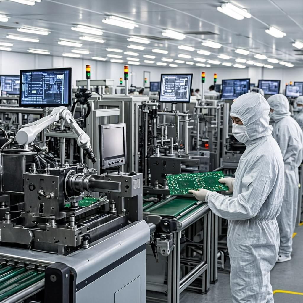
Miniaturized electronic circuit boards are used in various industries: consumer electronics, communication systems, the automotive and aerospace industry, the healthcare sector, etc. In all these industries, high-density PCBs, otherwise called high-density interconnects (HDI PCBs), are of critical importance. HDI technology enables smaller-footprint devices to be produced at a competitive cost without compromising quality, performance, or board reliability.
Any printed circuit board that offers dense placement of components and denser interconnections can be regarded as a high-density PCB or high-density interconnect (HDI) PCB. These PCBs offer higher wiring density per unit area compared to traditional PCBs.
High-density PCBs consist of:
With these features, high-density boards are compact and establish smaller dimension boards with smaller pads, vias, spaces, and traces. The high wiring density in HDI boards makes them lightweight, miniaturized circuits with a lower number of layers. With all these features, it is worth replacing a few PCBs on a product with a single HDI board.
According to IPC 2226, HDI PCBs are boards with:
IPC 2226 HDI board structures
High-density PCBs are extensively used in consumer electronics such as touch screens, mobile phones, tablets, computers, digital cameras, laptops, etc. HDI boards are smaller than traditional boards, without compromising on performance. The advantages of HDI PCBs are:
Populating more components on either side of HDI PCBs leads to smaller footprints and lightweight boards with improved functionality.
With HDI technology, it is possible to reduce the raw material quantity, number of layers, and even the number of boards, which leads to an overall reduction in cost.
As components become closer and the number of transistors per unit area is higher, it is clear that the performance is improved in HDI boards. There are fewer signal integrity issues in HDI boards and a significant decrease in crossing delays, signal losses, etc. The use of micro vias over through holes has a remarkable impact on the reliability of the HDI board due to the former’s smaller aspect ratio and high-quality construction.
The HDI PCB production process exhibits outstanding design efficiencies and shortens the time to market. With HDI boards, design and testing also speed up.
Here are some other differences between HDI PCBs and standard PCBs.
High-density PCB designs will continue to replace standard PCB designs due to their advantageous features, and the technology of high-density PCBs will continue to evolve to improve the degree of compactness and miniaturization. Cadence OrCAD PCB Designer software offers comprehensive PCB solutions for designing HDI boards with advanced routing and component placement technology.
Leading electronics providers rely on Cadence products to optimize power, space, and energy needs for a wide variety of market applications. If you’re looking to learn more about our innovative solutions, talk to our team of experts or subscribe to our YouTube channel.
Cadence PCB Education is a knowledgeable writer and educator specializing in PCB design and analysis. With a strong focus on bridging the gap between academic theory and practical application, Cadence PCB Education creates engaging, accessible content tailored to the needs of students and professors alike. Their work covers a wide range of topics, from foundational principles of PCB design to advanced analysis techniques, helping learners build a solid understanding of electronic engineering concepts. By breaking down complex ideas into clear, digestible insights, Cadence PCB Education empowers students to excel in their studies and supports professors in delivering impactful lessons.
Evaluate how our PCB software fits in your design workflow.