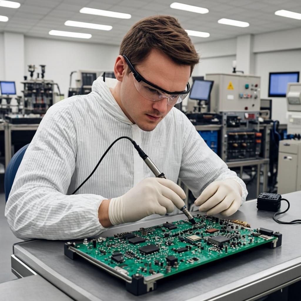
PCBs are no longer new, but their importance in electronics cannot be overstated because they make it possible to organize large circuits and components in a tiny space. Without them, miniaturized electronics like smartphones and smartwatches would be impossible to build.
However, to pack this large circuit in a tiny space, you have to handle heat, interference, impedance, and other electrical and physical factors carefully to make it work. So, the entire production process, from PCB design to PCB manufacturing and component assembly, must be carefully handled.
In this guide, we’ll focus on PCB design and fabrication processes to show you how the process should be handled to the end. Let’s get right into it!
The PCB production process begins with design, and it’s crucial to select the right design software. This choice helps you:
Considering these factors is essential for choosing the right software for your project.
The software should offer features like a comprehensive component library, which can reduce design time by eliminating the need to import external parts. It should also support multiple layers to facilitate complex PCB designs, board simulation to identify potential issues (such as components placed too close together), design rule checking, and 3D modeling with zoom capabilities for both bird’s eye and close-up views of all features.
With the right software, the PCB production process becomes much smoother, ensuring accuracy and efficiency in bringing your designs to life.
Overall, the more features the software has, the more powerful and capable it is for handling different PCB design projects. Some options worth checking out include Altium Designer, Autodesk Eagle, and DipTrace.
The two factors to consider here are an intuitive user interface and a short learning curve so that you can get the ball rolling in a short time. But don’t sacrifice features for a short learning curve. Always place the feature set before ease of use.
Check the design software’s capability to integrate with other CAD tools, as well as its support for different file formats. The broader its integration and compatibility, the smoother your workflow will be.
The last factor is cost. Advanced PCB design software can be expensive, especially when you factor in multi-user licenses and add-ons. But there are cheaper alternatives, although some might not be of the best quality. So, compare the features and quality first, then narrow down your list using the cost factor. You can use this guide as a start.
First, depending on the purpose of the PCB you are designing, you must consider the size and shape of the board.
The board is a primary component of the PCB because it holds all the other parts. Factors determining the size and shape of the PCB include the functionality and size of the destination product.
For example, wearable products such as activity trackers require way smaller PCBs than televisions.
As for component placement, consider the manufacturing of the PCB because that is the end goal. For instance, similar components, such as transistors, should face the same direction when placed for easier installation and inspection by the manufacturer.
Keep in mind the size and height of each component. Some components will be larger than others, which may result in uneven bumps on the circuit board when placed next to each other.
Some taller details may block shorter elements, and when the board is passed through the soldering oven to engrave the parts onto the board, it may return with poorly connected solder joints.
Always consider the height and width of components on the board – details of similar dimensions can be placed towards one side, ensuring the soldering wave reaches the smaller parts without being blocked.
Also, leave space for routing. If you place components too close together, you will run out of reach when you start routing. Integrated circuits, for example, have lots of pins to be connected around the board. To prevent running out of space and jumping over your design layout again, give enough room for components that require lots of pins to be connected to make the process easy.
Consider these techniques when routing the traces.
Remember to establish the ERC (Electrical Rules Check) and DRC (Design Rules Check) guidelines for quality control purposes during design to ensure the manufactured board is functional and error-free. They include defining physical requirements like trace and gap widths, via-hole selection for different nets, and high-speed electrical requirements to automate the PCB layout review to validate the layout.
Set these rules before beginning the design and layout processes, and run them throughout the design process to help identify and rectify potential issues early on. Running the rules at the end of the design process can highlight multiple errors that require tons of rework, which will waste time.
PCB stack-up forms the foundation of the entire PCB. It involves placing insulating and copper layers and laminating them with an adhesive. The stack comprises the various layers within the PCB and allows you to establish the characteristic impedances at each layer. But the more layers the PCB has, the costlier it becomes.
The top layer is the silkscreen that adds other indicators, such as letters and symbols, to the board, while the bottom layer is the substrate/dielectric (usually FR4), which gives the board its rigidity and thickness.
The ones in between are the copper layer for conductivity and the solder mask, which gives the PCB its distinctive green color and protects the copper from oxidation.
Optimal multilayer stacking cuts off external noise, enhances the design’s electromagnetic compatibility, keeps the cost within budget, and ensures efficiency in the manufacturing technique.
The material that usually varies depending on the application, thermal performance, and cost is the dielectric. FR4 is the most commonly used one because it is relatively cheap. However, since it is a fiberglass material, it isn’t a good conductor of heat.
For circuits with hot components like LEDs, metal is the better alternative because it dissipates heat quickly while providing structural strength as well. Metal also has a higher glass transition temperature, so it won’t deform when temperatures rise. The most commonly used one is aluminum.
However, metal is also electrically conductive, so there must be an insulation layer between the substrate and the circuit, which reduces heat dissipation. So, another alternative for PCBs with extremely hot components is ceramic. But ceramic is very expensive, so metal is the preferred option.
A PCB via-hole allows interconnections between different layers of the board. Vias may join traces, pads, and other conductive elements and provide the path for electrical and thermal energy moving from one layer to another.
Since we drill holes through the board to create the vias, you must consider each hole’s placement and size in relation to the other PCB components.
Ensure all the vias on the board are the same size to improve efficiency in the manufacturing process.
There are three basic types of vias: through vias, blind vias, and buried vias. Through vias connect two visible exterior layers. But blind vias connect a visible outer layer with an invisible interior layer, while buried vias connect two hidden interior layers.
Other vias include thermal vias for transferring heat from the top layer to the bottom or internal layers and tented vias enclosed with solder masks to prevent electrical and thermal components leakage.
Be sure to discuss the capabilities of the via types you intend to use with your PCB manufacturer because different vias have different heat and current-carrying capacities.
Thermal issues affect larger circuit boards with higher density and excessive processing speeds. To avoid such problems, your PCB must allow heat to dissipate.
During the material selection, identify components generating a lot of heat and find ways of diverting heat from them. The surface space around parts quickly becoming hot is a crucial layout design consideration because they’ll need space to cool off.
You may consider including heat sinks, cooling fans, and thermal reliefs.
Some places to add thermal reserves include through-hole vias to slow the heat sinking rating through the PCB layers.
A Gerber file contains information that guides the production of a PCB. As you might have observed, the Gerber file format is a de facto standard that defines 2D binary images using open ASCII vector format.
Modern Gerber files may also include metadata (data about other constituting data within a file) like solder mask, legend/silk, and number of copper layers, among other relevant printing information.
PCBs are made from Gerber 274-X data and NC drill files.
Each Gerber file corresponds to one layer in the physical board – the component overlay, top signal layer, bottom signal layer, solder masking layers, inner layers, etc.
This file format is important because, in 2015, UCAMCO estimated that about nine in every ten PCB productions are pres