With LEDs as well, most of the electrical power is converted to heat rather than light. This thermal loss must be dissipated to ensure reliable and stable LED operation for exploiting the complete performance and efficiency of the LEDs. Because of the trend towards miniaturization, thermal output per surface unit is increasing, which means that ever increasing heat is emitted onto an ever smaller surface area for dissipation.
Heros Electronics is a LED PCB supplier, which provides LED PCB manufacturing and LED PCB assembly service with excellent manufacturing and assemblying work flow, experienced workers and advanced equipment.
With high-power applications, sufficient thermal management is thus of central importance. In general, many options exist to achieve this, although these depend on the specific application and ambient conditions. A universal, optimal design or concept is not realizable for this reason, but has to be individually designed according to the specific assembly, specific requirements and the complete system. A principal overview of PCB technologies available on the market and their suitability for LED applications is outlined as below,
As a support element with direct contact to the components, the PCB is in certain respects the primary component for achieving thermal management. Making mistakes here with insufficient optimization means that resultant disadvantages at other locations in the complete system must be compensated for by measures that increase costs. For this reason the following fundamental considerations must be made beforehand:
The selection of appropriate materials for the circuit board is therefore of the utmost importance.
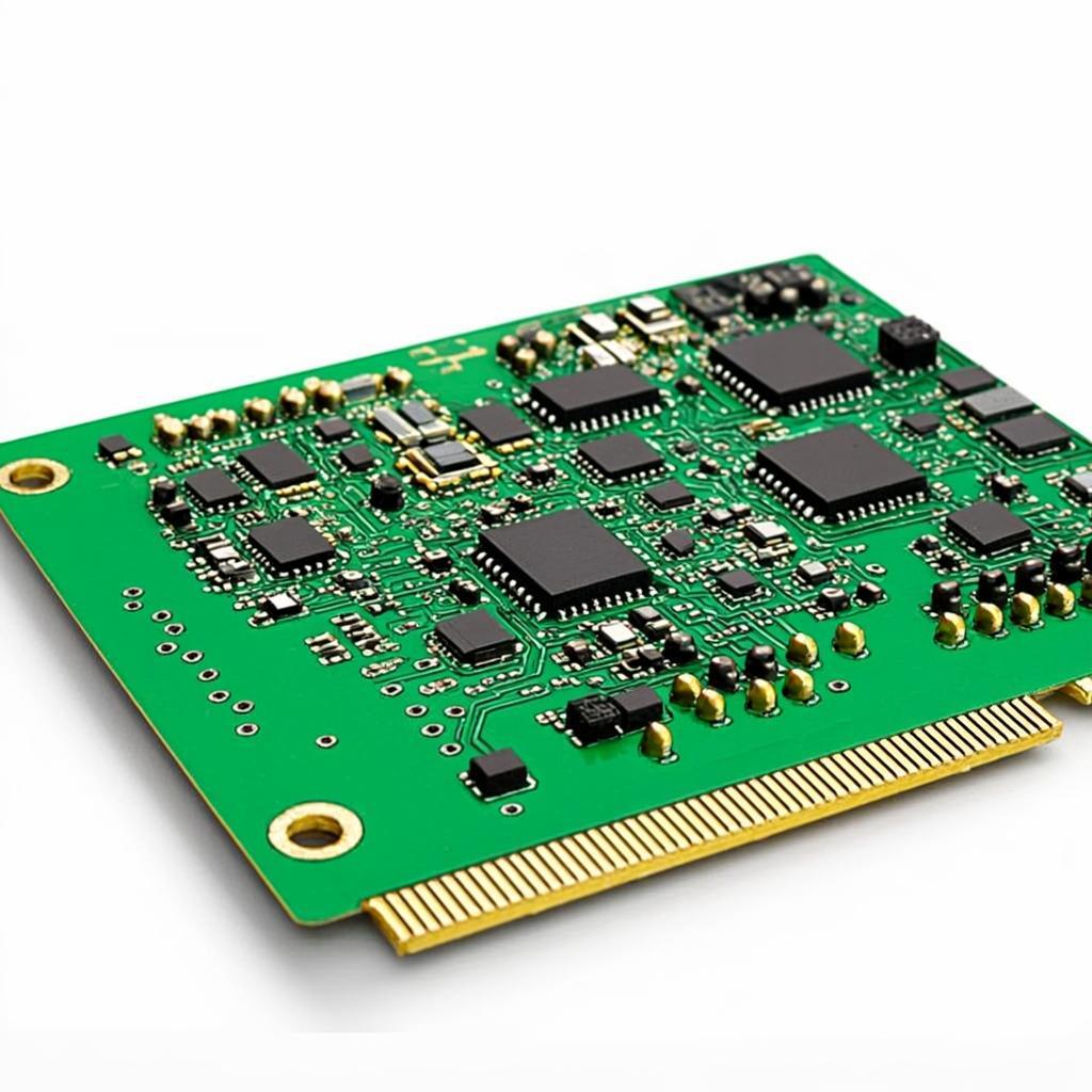
Classic composite PCB of glassfiber and expoxy resin, available in various compounds, versions (single-/multilayer) and thickness (0.3-3.5mm)
Thermal Distribution occurs here in the copper layer (typical thickness 35 μ m) on the PCB surface via heat distribution. Thicker copper layers (e.g. 70 μ m & 105 μ m) improve thermal dissipation properties and thus enable heat distribution over larger surfaces.
Fig. 1: Schematic diagram of a single-sided FR4 PCB
Pure standard substrates without improvements such as FR4 are normally not suitable for use with high-power LEDs due to their low thermal conductivity (0.2-0.5W/m*K).
Thin double-sided FR4 material with plated through-holes (=thermal vias) to ensure a thermal path through the FR4 substrate and to improve heat conduction. The thickness of the PCB is typically in the range of 0.3mm ≤t ≤1.0mm.
Fig. 2: Example of an FR4 PCB with thermal via arrays
The vias take on the heat transport function here, thus significantly improving vertical thermal resistance of the FR4 material in a targeted and localized manner. The thermal conduction capability of the vias themselves is determined by the thickness of the copper in the through-holes, via diameter and via pitch. Standard copper thickness of 20-25 μ m have become established in the industry, but greater wall plating thickness are also used. As a general rule, the thicker the copper layer, the better the performance–but also costs increase with thickness.
Two types of thermal via are possible:
Fig 3: Schematic layout of a thermal via
The use of thermally conductive silver pastes for filing to improve the thermal conductivity of the vias has in practice only a minor thermal effect but increase costs. For economic reasons it is thus better to slightly enlarge the copper thickness in the hole.
Fig 4: Schematic diagram of an OSLON LED on an FR4 PCB with plugged & filled vias
The filled, copper-capped vias have the important advantage that they can be arranged directly under the thermal solder pad of the LED (e.g. OSLON, Golden DRAGON, OSLON Black Flat, etc.), meaning they are able to directly conduct heat. The copper plugging prevents uncontrolled solder wicking / solder voiding during reflow soldering at open vias (solder run-off).
Fig. 5: Unfilled thermal vias have solder wicking if used in solder pads
Uncontrolled solder wicking generates solder balls on the backside of the PCB (Fig. 5), leading to insufficient thermal connection between the PCB and the heat sink.
In many cases however, simple thermal vias are sufficient to achieve a clear reduction in thermal resistance down to the targeted value. The level of resultant thermal resistance is affected by the number and position of the vias. The closer the vias are located to the heat source, the better and more quickly can heat be dissipated and the lower the thermal resistance (Fig. 6).
Fig.6: Comparison of the effect of two different configurations of thermal vias (simulation)
As a general rule it is advisable to design the copper surface around the solder pads, especially at the thermal pad if existing, to be as large as possible in order to achieve sufficient heat distribution across the FR4.
Thick copper PCBs are with copper layer thicknesses of 105 μ m to 400 μ m, and up to 500 μ m in special cases, According to requirements and technology used, ayers are applied in a planar way as extemal and/or internal layer. T he basis material used is FR4 or a metal substrate (Al, Cu) with a dielectric.
The primary application sector consists of applications with high power (high current) and for the cooling of components with large thermal power losses. Constructions are mainly multi-layer or double-sided PCBs.
Fig. 7: Schematic diagram of a copper thick-layer PCB
A special form is the so-called “iceberg”technology. Here a thin-layer copper layout os combined with selectively applied thick copper layers. The thick layer areas are recessed into the basis material (FR4) to achieve a uniform surface level. Expanding the copper cross-section achieves significantly wider heat dissipation as well as enabling local thermal build-up to be controlled.
The base materials of FR4 technology are used here, in which application-specific copper wres and/or copper profiles are integrated and connected to the connection surfaces.
Fig. 8: Schematic PCB diagram with integrated copper wire/profile
Fig. 9: Typical layer construction of an insulated metal substrate PCB
Expansion of the copper cross-section favors thermal distribution, and heat can be specifically dissipated due to the individual position in the PCB. Typical copper cross-sections are for example: 2mm x 0.5mm, 4mm x 0.5mm.
Insulated metal substrate (IMS) is the term for a PCB constructed with a metallic support plate separated by a thin dielectric from the copper conductors of the circuit. Aluminum is usually used as a carrier material because of low costs, and copper is also used with higher power densities because of its superior thermal conductivity, The attached dielectric has significant influence on total performance and is the determining factor for thermal resistance. Layers of unfilled and filled epoxy resins are used.
With filled resins, 3 to 10-fold higher thermal conductivity is achieved compared to FR4 depending on filling material and quantity, but filling materials influence the cycle resistance of the board. Layer thickness of the dielectric is in the range of 0.02mm to 0.1mm, although the fact that decreasing thickness of the layer usually leads to a reduction of electrical dielectric strength must generally be taken into account.
However, based on the structure, the IMS is mostly single-layer. Multi-layer versions are available but with higher costs.
In most applications IMS boards are attached to the heat sin together with a thermal interface material (TIM) by screws. When using an IMS-PCB with ceramic based LEDs, it should be considered that the difference in the coefficients of thermal expansion (CTE) between the ceramic material of the LED and the IMS PCB creates stress on the solder joint.
To minimize this effect, copper (Cu) is therefore preferred to aluminum (Al) as base plate material because of its lower CTE. Due to its significant higher thermal conductivity compared to FR4 technology (~ factor 10), IMS is widely-used in LED applications, especially with high power LEDs. In terms of material prices, costs with IMS can be approximately 2 to 4 times higher than with FR4.
This is an optimized variant of IMS PCBs where the metal of the metal plate partially protrudes through the insulation layer(Exposed Cu). The housing is partly directly connected to the metallic carrier here for bridging the dielectric.
Fig. 10 LED on PCB with exposed copper
Here heat can be dissipated without requiring any insulation between the thermal pad, the metal layer and the heat sink.. This permits LEDs to be operated at higher currents or higher power levels for example. It should be generally considered here that the connected thermal contact points are electrically new neutral. In combination with ceramic based packages however, some PCB designs with exposed copper may cause higher thermal mechanical stresses during the assembly process. Because of this, application designs need to be verified to avoid damage. Please confer with application team.
This is a modified form of IMS technology. Instead of a dielectric made of epoxy resin, a thin aluminum oxide or ceramic layer is used. Depending on the required dielectric strength, the dielectric layer thickness is in the range of <0.04mm to 0.125mm, whereby thermal conductivity of approximately 2W/mK is achieved.
Fig. 11: Schematic PCB diagram of aluminum with thin insulation layer
The core of the PCB here is a ceramic carrier substrate to which the conductors are directly applied via thick film or thin film technology. According to the specific variant, ceramic carriers have thicknesses of 0.25mm to 3mm. Because ceramic substrates themselves are electrically insulating but are thermally conductive, heat can be dissipated directly without other thermal barriers.
Aluminum oxide and aluminum nitride are usually used as substrate materials, the later having significantly superior thermal conductivity properties. The thermal conductivity of aluminum oxide is in the range of ~20-25W/mK, and that of aluminum nitride is at (~170W/mK). Another advantage among many is low thermal expansion. In combination with ceramic-based hig-power LEDs, they are thus primarily suitable for applications with high thermal cyclic loads. With regard to thermal management, ceramic PCBs are generally very effective, but are often seen as a luxury variant because of their higher costs.
In general, all finishes are well-proven for SMT assembly, but with smaller solder pads the quality of the plating/finish is more important. Hot air solder leveling (HAL/HASL) finish is less preferred for assembly because of the uneven surface compared to completely“flat”platings such as Cu-OSP (Organic Solderability Preservative) or immersion Sn or NiAu (ENIG).
From a package point of view, it is difficult to recommend a particular PCB pad finish that will always meet all requirements. The choice of finish also depends strongly on board design, pad geometry, needs of other components on the board and process conditions, and must be chosen according to the needs of the specific application.
Internal tests show that Cu-OSP or ENIG (immersion Gold) are suitable and reliable plating in most cases.
Fig. 12: Comparison of PCB finishes
The term “second level reliability”usually appears in connection with the requirements and characteristics of the application or of the overall system (Fig.13). It ultimately however refers to the reliability of the solder connection between the component (e.g. LED) and the printed circuit board (PCB) or carrier substrate.
Fig. 13: Requirements and properties for efficient system design
The reliability of the soldered joint itself is determined or influenced by various factors, e.g. component housing, solder, mounting and soldering process and printed circuit board (Fig. 14).
Fig. 14: Influencing factors on 2 nd Board Reliability
This i