Flexible small-batch PCBA for prototypes and NPI: BGA down to 0.25 mm (zero point two five millimeter) pitch, DFM/DFT reviews, 3–10 day (three to ten day) quick-turn, and MES traceability. Smooth handoff to volume and box build.
Tight feedback loops from first articles to pilot runs
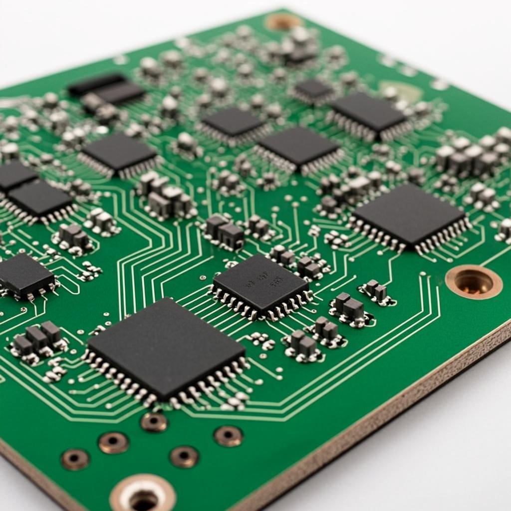
Small batch assembly bridges concept validation and market introduction. We combine rapid prototype turnaround with production-grade process controls—stencil optimization, 3D SPI (solder paste inspection), and closed-loop reflow profiling—to ensure your prototypes behave like scaled builds. Typical batch sizes range from 10–5,000 units (ten to five thousand), executed under the same process gates used for mass production.
Comprehensive DFM/DFT reviews flag spacing, thermal relief, and test-point accessibility before commitment. Assembly lines maintain first-pass yield (FPY) above 98% (ninety-eight percent) with DPPM below 500 (defects per million less than five hundred) through automated inspection and feedback loops. For reflow quality, we employ reflow profile optimization tuned by component thermal mass and verified through SMT assembly standards.
Critical Risk: Prototype runs often suffer from stencil aperture variation, paste slump, or thermal imbalance, causing tombstoning or solder voids that mask latent defects before scale-up.
Our Solution: We stabilize print and reflow performance using process characterization, X-bar/R control charts, and automated optical inspection with closed-loop corrections. Data from small-batch builds feed into predictive models for large-volume assembly and full box build, ensuring identical quality criteria from pilot to production.
For turnkey efficiency, our turnkey assembly framework integrates material sourcing, firmware loading, and test plan management—accelerating launch cycles while preserving documentation traceability across builds. For pricing transparency, see our PCB assembly quote guide.
Inspection and data capture at every critical step
AOI after placement prevents cascading defects; post-reflow AOI verifies joint quality. For BGA/QFN we add sample X-ray with void targets typically ≤25% (less than or equal to twenty-five percent) per IPC-7095. Through-hole uses selective or wave solder with documented preheat, contact time and temperature windows.
ESD handling follows ANSI/ESD S20.20 with continuous monitoring. Where needed, we add functional or boundary-scan tests; see our functional testing guide. Component sourcing can be kitted, partial or full turnkey via turnkey assembly while keeping single-source accountability.
Repeatable quality with upgrade path to volume
Whether you need simple prototypes or complex production runs, our advanced manufacturing capabilities ensure excellent quality and reliability. Get your quote within 30 minutes.
Use adequate keep-outs, consistent reference orientation, and balanced pads to avoid tombstoning. Test-point pads ~0.75 mm (about zero point seven five millimeter) with ~2.54 mm pitch (about two point five four millimeters) simplify fixtures. For BGA fan-out, manage via-in-pad with fill/planarization to prevent solder wicking. See our BGA assembly tips and assembly quote guide.
Flow: incoming inspection → stencil setup → paste print → 3D SPI → placement → reflow → AOI → sample X-ray → THT (if any) → final inspection and test. Typical reflow: ramp 1–3 °C/s (one to three degrees per second), TAL 60–90 s (sixty to ninety seconds), peak 245–250 °C (two hundred forty-five to two hundred fifty) for SAC305. Learn the fundamentals in our manufacturing guide and PCBA quality control.
Choose kitted, partial or full turnkey assembly. We track lifecycle and alternates to mitigate EOL risks. MSL parts follow J-STD-033 with dry-cabinet storage ~10–20% RH (ten to twenty percent) and baking at 125 °C (one hundred twenty-five) for 8–24 h (eight to twenty-four hours) as needed.
First-article reports capture dimensions and joints before release. Process data—SPI volume, placement offsets, reflow profiles—is logged with limits and alarms. Non-conformance tracking drives corrective actions. Documentation aligns with ISO 9001; for regulated programs we extend retention windows and add PPAP-style packages.
IoT and consumer devices prioritize speed-to-market (3–10 days). Medical prototypes add documentation and traceability under ISO 13485 practices. Automotive pilots include thermal cycling and vibration before PPAP. When designs mature, transition to large-volume assembly and enclosure box build.
Experience: hundreds of prototype/NPI ramps with stable FPY.
Expertise: fine-pitch stencil design, 3D SPI control, BGA X-ray criteria and selective solder tuning.
Authoritativeness: IPC-A-610/J-STD-001 workflows; see IPC standards mastery.
Trustworthiness: MES traceability from lot to unit with AOI/X-ray/test reports available on request.
Gerbers, BOM with MPNs and reference designators, pick-and-place (XY/Centroid), and assembly drawings for special notes. For turnkey, include acceptable alternates to reduce risk and lead time.
We optimize stencil apertures and verify paste volume with 3D SPI, then use sample X-ray to check voids and alignment. Via-in-pad is filled and planarized to prevent solder wicking.
Yes. We support boundary-scan, power-on and custom fixtures. See the overview of functional testing for coverage choices.
Typical quick-turn is three to ten working days depending on complexity and materials. Express options exist for critical paths once DFM is cleared.
From simple prototypes to complex production runs, our world-class factory delivers superior quality, fast turnaround and competitive pricing. Join thousands of satisfied customers who trust us with their PCB manufacturing needs.