Helen Frankenthaler PCB Circuit Board R&D Center

intelligent toilet pcba wiring diagram

Smart Toilet Monitoring PCB Solution

Introduction to Smart Toilet Monitoring Systems

Smart toilet monitoring systems represent a significant leap in hygiene, health management, and operational efficiency, integrating advanced sensor technologies and data analytics to transform a basic utility into an intelligent health and environmental hub. At the core of these sophisticated systems lies the Printed Circuit Board (PCB), acting as the central nervous system that orchestrates all functionalities, from precise water temperature control and automatic flushing to comprehensive health data collection and remote diagnostics. These PCBs are meticulously engineered to withstand the unique environmental challenges of a bathroom, ensuring reliable, long-term performance and enabling seamless interaction between various smart components.

Defining Smart Toilets

Smart toilets are advanced sanitary fixtures equipped with integrated electronic systems that offer enhanced functionalities beyond basic sanitation. These often include automated flushing, bidet functions with adjustable water temperature and pressure, heated seats, air deodorizers, and self-cleaning mechanisms. Crucially, many modern smart toilets incorporate health monitoring capabilities, such as urine analysis or vital sign measurement, providing users with actionable insights into their well-being.

Key Functionalities of Smart Toilet Systems

Beyond convenience features, smart toilet monitoring systems excel in providing proactive maintenance alerts, optimizing water usage through intelligent sensing, and enhancing user comfort through personalized settings. For commercial and public spaces, these systems can monitor usage patterns, detect leaks, and provide real-time status updates, significantly reducing operational costs and improving hygiene standards. The ability to collect and transmit data wirelessly is fundamental to these functionalities.

The Pivotal Role of PCBs

PCBs are indispensable to smart toilet systems, serving as the foundational platform for integrating diverse electronic components. They facilitate the precise control of mechanical actuators, the accurate reception and processing of sensor data (e.g., occupancy, water levels, bio-signals), and reliable communication with external networks (Wi-Fi, Bluetooth). The design of these PCBs must consider miniaturization, robust environmental protection against humidity and water, efficient power management, and electromagnetic compatibility (EMC) to ensure flawless operation in a demanding environment.

The advancements in PCB technology are directly correlated with the evolution of smart toilet capabilities, enabling more compact, powerful, and reliable systems. As a leading PCB solution provider, Zero One Solution Limited specializes in developing robust and highly integrated PCBs that meet the stringent requirements of smart toilet monitoring systems, paving the way for healthier and more efficient sanitary solutions globally.

Key Components of a Smart Toilet Monitoring PCB

The efficacy and intelligence of any smart toilet monitoring system are fundamentally rooted in the sophisticated design and integration of its Printed Circuit Board (PCB). This intricate core orchestrates all functionalities, from advanced hygiene features to health monitoring capabilities. Understanding the critical components within a smart toilet monitoring PCB is paramount to appreciating the complexity and innovation driving these cutting-edge devices.

Component CategorySpecific ComponentsFunction in Smart Toilet PCB
SensorsPressure Sensors, Temperature Sensors, Proximity Sensors, Flow Sensors, pH SensorsDetect occupancy, water temperature, user presence for auto-flush/seat warming, water usage, and analyze biological samples for health insights respectively. They are crucial for data acquisition, enabling features like automatic flushing, bidet control, and health monitoring.
Microcontrollers (MCUs)ARM Cortex-M Series (e.g., STM32, ESP32)The brain of the smart toilet, processing data from sensors, executing control logic for actuators (e.g., bidet nozzles, dryers), and managing communication. They enable complex algorithms for personalized settings and diagnostics.
Communication ModulesWi-Fi (IEEE 802.11), Bluetooth Low Energy (BLE), LoRaWAN (for specific applications)Enable connectivity to smart home networks, mobile applications, and cloud platforms for data logging, remote control, and firmware updates. Wi-Fi offers high bandwidth for rich data, while BLE provides energy efficiency for specific interactions. LoRaWAN extends range for broader IoT integration.
Power Management CircuitsVoltage Regulators (LDOs, DC-DC Converters), Battery Management ICsEnsure stable and efficient power distribution to all components. They manage power conversion from AC or battery sources, optimize energy consumption, and protect against power fluctuations, critical for reliability and energy efficiency.
ActuatorsMotor Drivers, Solenoid Drivers, Heater Control CircuitsTranslate electrical signals from the MCU into physical actions, such as controlling the bidet spray, operating the air dryer, flushing mechanisms, and heating elements for seat warming or water temperature control.
  • Why are low-power components critical for smart toilet PCBs? Low-power components are crucial for smart toilet PCBs primarily to reduce energy consumption, especially in battery-backed or always-on systems. This minimizes operational costs, enhances environmental sustainability, and can extend the lifespan of components by reducing heat generation. Efficient power management also allows for more compact designs by reducing the need for large heat sinks or complex cooling solutions, directly impacting product form factor and cost.

Design Considerations for Smart Toilet PCBs

Designing Printed Circuit Boards (PCBs) for smart toilet monitoring systems demands meticulous attention to specific considerations to ensure optimal performance, longevity, and user safety. The inherent environment of a smart toilet system, characterized by confined spaces and fluctuating environmental conditions, necessitates a sophisticated approach to PCB layout, material selection, and component integration. These critical design considerations are paramount in developing a reliable and efficient smart toilet PCB solution.

  • Miniaturization and Size Constraints Smart toilets typically have limited internal space, requiring highly compact and space-efficient PCB designs. This often involves using high-density interconnect (HDI) PCBs, micro-vias, and smaller surface-mount components (SMCs) to maximize functionality within a minimal footprint. Strategic component placement and optimized routing are essential to achieve the required compactness without compromising performance.
  • Power Efficiency and Management Many smart toilet features, such as continuous monitoring and rapid response, necessitate efficient power management. The PCB design must incorporate low-power components, efficient voltage regulators, and intelligent power-saving modes to minimize energy consumption. This is crucial for both sustainability and reducing operational costs, especially for devices that may be always-on or frequently activated.
  • Signal Integrity and EMI/EMC Maintaining signal integrity is critical for accurate sensor readings and reliable communication within the smart toilet system. Designers must employ careful trace routing, impedance matching, and grounding techniques to prevent signal degradation and cross-talk. Furthermore, the PCB needs to be robust against electromagnetic interference (EMI) and ensure electromagnetic compatibility (EMC) to prevent interference with other electronic devices and ensure stable operation in a potentially noisy environment.
  • Environmental Durability (Humidity, Temperature, Water Resistance) The bathroom environment exposes PCBs to high humidity, temperature fluctuations, and the potential for water splashes. Therefore, the PCB materials must exhibit excellent moisture resistance, and components should be selected for their operational range within these conditions. Conformal coatings, hermetic sealing, and appropriate enclosure designs are often employed to protect the PCB from moisture ingress and ensure long-term reliability in such challenging environments.
  • Sensor Integration and Accuracy Smart toilet PCBs integrate various sensors (e.g., proximity, temperature, pressure, chemical). The design must ensure proper sensor placement, noise reduction, and dedicated signal conditioning circuits to achieve high accuracy and responsiveness. The PCB layout should minimize interference between different sensor types and their associated circuitry.
  • Thermal Management Despite low power consumption, certain components can generate heat. Efficient thermal management, including proper heat dissipation pathways and potentially heat sinks, is important to prevent overheating and ensure component longevity and stable performance, especially in confined spaces with limited airflow.

PCB Manufacturing and Assembly Process

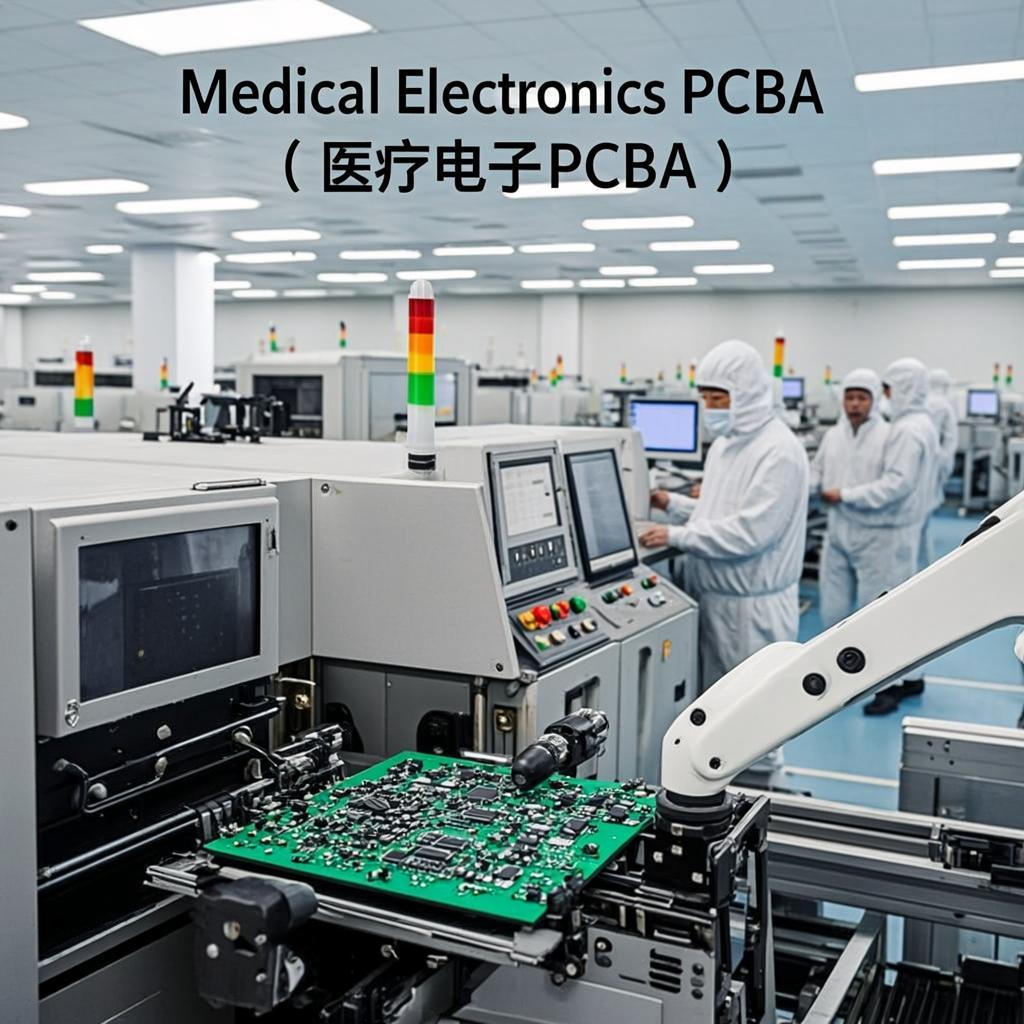
The manufacturing and assembly of Printed Circuit Boards (PCBs) for smart toilet monitoring systems demand precision and adherence to stringent quality standards, given the product's long lifespan and sensitive operating environment. This intricate process transforms a digital design into a functional electronic heart, ensuring the seamless operation of a smart toilet's advanced features, from sensor data acquisition to complex control logic. Zero One Solution Limited leverages its state-of-the-art facilities and expertise to deliver high-quality, reliable PCBs that meet the unique requirements of smart toilet applications.

Process StageDescriptionKey Considerations for Smart Toilet PCBs
Material SelectionChoosing the right substrate (e.g., FR-4, high-Tg laminates) and copper foils.Moisture resistance, thermal stability for prolonged use, lead-free compatibility, cost-effectiveness vs. performance balance.

The fabrication techniques employed are critical for the durability and performance of smart toilet PCBs. These include precise etching for circuit traces, multi-layer lamination for compact designs, and advanced drilling for component placement. Following fabrication, the assembly process integrates all electronic components onto the bare PCB. This typically involves Surface Mount Technology (SMT) for smaller components and Through-Hole Technology (THT) for larger, more robust parts. Automated pick-and-place machines ensure high accuracy and speed, while reflow soldering or wave soldering techniques create reliable electrical and mechanical connections. Rigorous quality control, including Automated Optical Inspection (AOI) and X-ray inspection, is performed at various stages to detect any manufacturing or assembly defects, guaranteeing the final product's integrity and reliability in a humid and demanding environment. Our comprehensive approach ensures that every PCB delivered is ready for seamless integration into sophisticated smart toilet systems.

Rapid Prototyping for Smart Toilet PCB Solutions

Rapid prototyping is a critical enabler in the accelerated development cycle of Smart Toilet Monitoring PCB Solutions, allowing for swift iteration, validation, and refinement of designs. This agile approach minimizes time-to-market and significantly reduces overall development costs by identifying and rectifying potential issues early in the process. Zero One Solution Limited excels in providing rapid prototyping services, ensuring that innovative smart toilet concepts transition from conceptualization to tangible, testable hardware with unprecedented efficiency.

  • Why is rapid prototyping essential for Smart Toilet PCBs? Rapid prototyping for Smart Toilet PCBs is crucial because it enables quick validation of complex sensor integrations, intricate power management circuits, and communication modules in a real-world environment. This iterative process allows engineers to detect and correct design flaws, optimize performance, and ensure reliability in challenging, high-humidity environments before committing to mass production, thereby saving significant time and resources and mitigating risks associated with late-stage design changes.
  • How does Zero One Solution Limited achieve quick turnaround times for PCB prototypes? Zero One Solution Limited achieves quick turnaround times through a highly optimized, integrated workflow that encompasses in-house design capabilities, automated manufacturing processes, and