In the electronics manufacturing industry, PCBs (Printed Circuit Boards) serve as the “skeleton” for electronic components, and the efficiency and quality of their mass production directly impact a product’s cost and reliability. Compared to small-batch prototyping, mass production requires a focus on consistency while managing costs and boosting efficiency. This involves multiple aspects, including design optimization, supply chain management, and process control. This article will provide a comprehensive breakdown of the key stages and practical considerations for mass-producing PCBs, from initial preparation to final testing.
The successful launch of mass production relies on “upfront preparation,” which accounts for over 60% of the effort. This stage involves aligning three core areas: design for manufacturability, material stability, and supplier compatibility. This is crucial to avoid cost overruns or quality issues that can arise from small oversights in a large-scale production run.
While small-batch prototyping might tolerate minor “design flaws,” in mass production, a tiny design issue (like a trace that’s too narrow) could lead to an entire batch being scrapped. Therefore, it’s essential to perform a comprehensive DFM (Design for Manufacturability) review of your PCB design, with a focus on these points:
For mass production, materials must not only meet performance standards but also have consistent batch-to-batch quality. For example, a 0.2 dielectric constant deviation in one batch of substrates could destabilize the signal in an entire run of communication devices. When selecting materials, focus on:
Mass-producing PCBs requires a supplier with stable delivery capability, not just the lowest price. When screening, you should verify three dimensions:
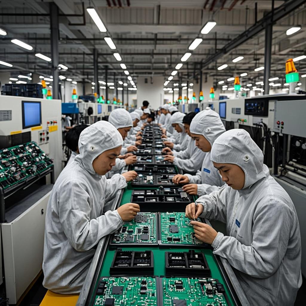
The process for mass-producing PCBs is similar to that of small-batch runs (cutting → drilling → pattern transfer → etching → solder mask → surface finish → shaping), but it requires using “equipment automation + parameter standardization” to boost efficiency and consistency. Each stage has specific points that are unique to large-scale production and require close monitoring.
Cutting is the first step in production, and it’s essential to control both “dimensional tolerance” and “material waste.”
Drilling quality directly impacts subsequent component insertion and soldering. In mass production, the key is to control “hole position accuracy” and “drilling efficiency.”
Pattern transfer “replicates” the design onto the substrate, while etching “removes excess copper foil.” These two processes must be controlled together to prevent “incomplete traces” or “over-etching.”
The solder mask (green oil) is the “protective layer” for the traces, and the silkscreen provides “assembly guidance.” Both need to have “uniformity” and “clarity.”
The surface finish should be chosen based on the “soldering process” and “storage requirements,” and mass production requires ensuring “uniformity of application.”
Shaping involves cutting the panel into individual PCBs, controlling “dimensional tolerance” and “board edge quality.”
Mass production PCB quality control must shift from “post-production inspection” to “in-process intervention.” It uses “in-line inspection + batch traceability” to ensure “early detection of defects and traceability of issues.”
Set up “three-level AOI inspection” after drilling, after etching, and after the solder mask process.