The world of electronics design is intricately woven with the art and science of Printed Circuit Board (PCB) layout. PCBs serve as the backbone of countless electronic devices, from smartphones to spacecraft, and the way they are designed and manufactured significantly impacts the performance and reliability of these technological marvels. In this comprehensive exploration, we will unravel the multifaceted realm of PCB layout, shedding light on the vital interplay of solder, PCB manufacturing processes, stack-up configurations, solder mounts, and board layout, as these elements converge to shape efficient and reliable electronic systems.
The layout of a PCB is akin to a meticulously crafted blueprint, providing a comprehensive map that precisely dictates the placement of essential electronic components such as resistors, capacitors, and integrated circuits (ICs). It serves as the architectural canvas where the intricate symphony of electrical connections unfolds. This intricate design blueprint not only governs the locations where these components must reside but also delves into the intricacies of how they harmoniously interact with each other through an intricate network of conductive tracks and pads. These conductive pathways are the lifeblood of any electronic system, transmitting signals and power to ensure the seamless operation of the device.
In essence, a PCB layout is not just a design, but a complex map that guides the functionality of an electronic device. This process demands a profound understanding of electronic components, circuit theory, and design principles. Therefore, the role of a PCB designer is pivotal in the electronics industry. They must possess a strong foundation in electronics, be proficient in PCB design software, and have an acute attention to detail to ensure that the layout is not only accurate but also highly efficient in serving its intended purpose.
PCB design is a complex process that involves several stages, from conceptualization to final production. It begins with the creation of a schematic diagram, which is a symbolic representation of the circuit. This diagram includes all the components that will be part of the circuit and their interconnections. The schematic serves as the guide for the PCB layout, which is the physical representation of the circuit.
The role of a PCB designer is multifaceted. They are responsible for translating the schematic into a functional PCB layout. This involves deciding the placement of components, routing the interconnections, and ensuring that the design adheres to industry standards and guidelines. The designer must also consider factors such as the electrical requirements of the circuit, the physical constraints of the PCB, and the manufacturing process.
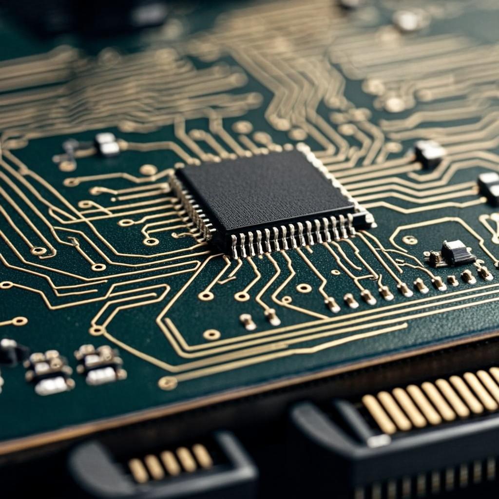
A PCB is composed of several components, each serving a specific function. The primary component is the board itself, which is typically made of non-conductive material like fiberglass or plastic. This board serves as the base upon which other components are mounted.
Resistors are common components found on a PCB. They regulate the flow of electricity through the circuit by providing resistance. The value of a resistor, measured in ohms, determines how much it resists the flow of current.
Capacitors are another type of component. They store and release electrical energy, acting somewhat like a battery. Capacitors are crucial for filtering noise from the power supply, blocking direct current (DC) while allowing alternating current (AC) to pass, and for many other functions.
Integrated Circuits (ICs) are essentially miniaturized circuits themselves that perform specific functions. These can range from simple logic gates to complex microprocessors. ICs are typically the most complex components on a PCB and often dictate the overall functionality of the device. The conductive tracks and pads are what connect all these components. These tracks, often made of copper, are etched onto the board in the design process. They provide the path for electrical current to flow between components. Pads are small portions of exposed metal where components are soldered onto the board. Each of these components plays a crucial role in the overall function of the PCB. The layout and interconnection of these components determine how the circuit performs and how the electronic device operates.
PCBs come in various types, each suited to different applications based on their physical and electrical properties.
Single-sided PCBs are the simplest type. They have components on one side of the board and conductive copper tracks on the other. These are typically used in simple electronics where space and complexity are not significant concerns, such as in power supplies and radios.
Double-sided PCBs have conductive copper tracks on both sides of the board. This allows for a higher density of components and interconnections, making it suitable for more complex devices. The two sides are connected using through-hole technology, where holes are drilled through the board and filled with conductive material to create electrical connections.
Multilayer PCBs take this concept further by having multiple layers of conductive tracks separated by insulation. These can range from 4 to 12 layers, or even more in high-density designs. The layers are connected using vias, similar to double-sided PCBs. Multilayer PCBs are used in highly complex devices like computers and medical equipment, where space is at a premium and a high degree of electrical performance is required.
Rigid PCBs are made from a solid substrate material like fiberglass that keeps its shape. They are durable and can support heavy components, but they cannot bend or flex. These are commonly used in desktop computers and other stationary electronics.
Flexible PCBs, in contrast, are made from materials like flexible plastic or Kapton. They can bend and flex without damaging the circuit. This makes them ideal for use in devices like cameras and mobile phones, where the PCB needs to fit into a compact, irregularly shaped casing.
Each type of PCB offers unique advantages and challenges in terms of design, manufacturing, and application. The choice of PCB type depends on the specific requirements of the electronic device being designed, including its complexity, physical constraints, and performance requirements.
The process of creating a PCB layout is a multi-step endeavor that requires careful planning and execution. It begins with the creation of a schematic diagram, which is a symbolic representation of the circuit. This diagram includes all the components that will be part of the circuit and their interconnections. The schematic serves as the guide for the PCB layout, which is the physical representation of the circuit.
Once the schematic is complete, the next step is to translate this into a PCB layout. This involves deciding the placement of components, routing the interconnections, and ensuring that the design adheres to industry standards and guidelines. The designer must also consider factors such as the electrical requirements of the circuit, the physical constraints of the PCB, and the manufacturing process.
Schematic capture is a pivotal phase in electronic circuit design, representing the art of creating a schematic diagram that serves as the circuit's blueprint. This diagram encompasses all components, complete with their schematic symbols, which are key to understanding their electrical functions and connections. Specialized software simplifies this process, offering designers the means to seamlessly insert and arrange components and draw the all-important connections.
The schematic capture process requires a deep understanding of the circuit's functionality. The designer must know what each component does, how they interact with each other, and how they contribute to the overall function of the circuit. For example, a resistor might be used to limit the current to a safe level for a particular component, while a capacitor might be used to filter out noise from the power supply.
Once the schematic capture is complete, it is then used as the guide for creating the PCB layout. The layout process involves translating the schematic into a physical design, deciding where each component will be placed on the board, and routing the interconnections between them. This requires a careful balance of electrical requirements, physical constraints, and design rules to ensure a functional and manufacturable PCB.
Component placement is a pivotal phase in the PCB layout process, one that demands meticulous attention to detail and adherence to design rules and guidelines. The objective is to create a layout that optimizes electrical efficiency, conserves space, and aligns with design rules, all while harmonizing the integration of surface mount components, Allegro design software, and the intricacies of circuitry.
The placement of components on a PCB is governed by a multitude of factors, each contributing to the overall performance and reliability of the final product. Foremost, the designer must account for the electrical requisites of the circuit. Components sharing a common function or signal path should be thoughtfully grouped, minimizing interconnection lengths. This reduction serves to mitigate signal degradation and electromagnetic interference (EMI), fostering the circuit's integrity.
Thermal management takes center stage in this endeavor. Components that generate substantial heat, such as power transistors and voltage regulators, necessitate strategic placement in areas with ample airflow or proximity to heat sinks. This ensures efficient heat dissipation, safeguarding against overheating and upholding device reliability.
The physical constraints of the PCB and the components themselves also play a part in the component placement. Components with large footprints or that require specific mounting hardware may need to be placed in specific locations on the board. Additionally, components that need to be accessible for maintenance or adjustment, such as connectors or potentiometers, should be placed in easily accessible locations.
Design rules and guidelines, often dictated by industry standards or device-specific parameters, exert their influence. These rules encompass minimum spacing between components, clearance from board edges, and alignment with other components. Strict adherence to these principles guarantees a manufacturable PCB design that meets industry standards.
Routing is the process of connecting the components on a PCB through conductive tracks. These tracks, often made of copper, provide the path for electrical current to flow between components. Routing is a critical aspect of PCB layout design, as it directly impacts the performance and reliability of the circuit.
When routing a PCB, several factors must be considered. First, the designer must ensure that the routing adheres to the design rules and guidelines. These rules, which can include minimum track width, spacing between tracks, and clearance from board edges, ensure that the PCB can be manufactured reliably and efficiently.
Signal integrity stands as another paramount consideration in the routing phase, playing a pivotal role in the design of high-performance electronic circuits. Designers are tasked with safeguarding the integrity of signals as they traverse the PCB, and in this endeavor, signal layers and signal traces emerge as vital components of the equation. The designer must minimize the length of the tracks and avoid sharp bends, as these can cause signal degradation and increase the risk of electromagnetic interference (EMI). Additionally, high-speed signals and sensitive analog signals should be routed away from noisy components, such as switching power supplies, to minimize the risk of crosstalk and other signal integrity issues.
Power distribution is also a critical aspect of routing. The designer must ensure that the power supply tracks are wide enough to handle the required current and that they are routed efficiently to minimize voltage drops. Ground planes, which are large areas of copper connected to the ground, can be used to provide a low-impedance return path for currents and to improve the overall performance of the circuit.
Thermal management is another factor to consider when routing a PCB.