Helen Frankenthaler PCB Circuit Board R&D Center

lot pcb assembly 3d

Multilayer PCB Manufacturing & 4/6/8/10/12 Layers Pcb Fabrication | PCBBUY

Our Service

PCBBUY specializes in 1-22 layer PCB prototyping and medium to large-scale production.

We focused on solving slow delivery and procurement difficulties for complex, high-difficulty, special, and multilayer-count orders.

8 Layers Board

  • Size≤10*10cm
  • Board thickness 1.2-2.4mm, copper thickness1-3oz, minimum hole size 0.2mm, minimum trace width 3mil.
  • AOI
  • 100% flying probe test
  • Epoxy filled vias
  • Copper clad on hole

10 Layers Board

  • Size≤10*10cm
  • Board thickness 1.6-2.4mm, copper thickness1-10oz, minimum hole size 0.15mm, minimum trace width 3mil.
  • Pattern plating 70min
  • Buried via
  • HF
  • Transparent solder mask

12 Layers Board

  • Size≤10*10cm
  • Board thickness1.6-2.4mm, copper thickness1-10oz, minimum hole size 0.15mm, minimum trace width 3mil.
  • Buried via、Multistage impedance
  • Custom stackup、Support TG130/180
  • Multistage Impedance Control
  • Specific Stackup

Product Display

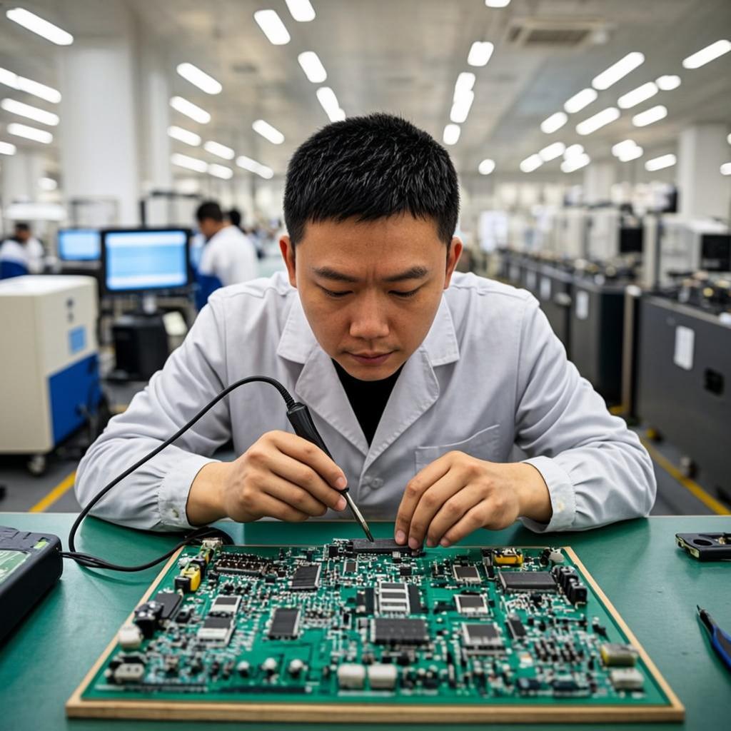
High quality & short lead time customized service for global customer over 100000+ choose us

  • 12 Layers Board Material: FR-4 Application: power system Layer/board thickness: 12/2.0mm Surface finish: ENIG Trace width/spacing: 3.00/3.00mil Mininum hole size: 0.2mm Technology: high TG, thick copper
  • 4 Layers Board Material: FR-4 Application: P2 sidplay screen Layer/board thickness: 4/1.6mm Surface finish: OSP Trace width/spacing: 3.00/3.00mil Mininum hole size: 0.2mm Technolugy: Tending via, high-precision
  • 4 Layers Board Material: FR-4 Application: Module boards set Layer/board thickness: 4/2.0mm Surface finish: ENIG Trace width/spacing: 8.00/8.00mil Mininum hole size: 0.4mm Technolugy: Multistage impedance control of inner & outer layer
  • 6 Layers Board Material: FR-4 Application: industrial control Layer/board thickness: 6/2.0mm Surface finish: HASL Trace width/spacing: 3.00/3.00mil Mininum hole size: 0.25mm Technolugy: vias not covered/copper thickness
  • 6 Layers Board Material: FR-4 Application: industrial electronics Layer/board thickness: 6/1.6mm Surface finish: ENIG Trace width/spacing: 3.00/3.00mil Mininum hole size: 0.3mm Technolugy: high-precision/ENIG
  • 8 Layers Board Material: FR-4 Application: CE Layer/board thickness: 8/1.6mm Surface finish: HASL Trace width/spacing: 4.00/4mil Mininum hole size: 0.2mm Technolugy: vias not covered/copper thickness
  • 8 Layers Board Material: FR-4 Application: intelligent printer Layer/board thickness: 8/2.0mm Surface finish: HASL Trace width/spacing: 3.00/3.00mil Mininum hole size: 0.2mm Technology: multistage impedance matching, high precision
  • 10 Layers Board Material: FR-4 Application: industry control Layer/board thickness: 10/2.0mm Surface finish: ENEPIG Trace width/spacing: 3.00/3mil Mininum hole size: 0.2mm Technolugy: ENEPIG
  • 12 Layers Board Material: FR-4 Application: power system Layer/board thickness: 12/2.0mm Surface finish: ENIG Trace width/spacing: 3.00/3.00mil Mininum hole size: 0.2mm Technology: high TG, thick copper
  • 4 Layers Board Material: FR-4 Application: P2 sidplay screen Layer/board thickness: 4/1.6mm Surface finish: OSP Trace width/spacing: 3.00/3.00mil Mininum hole size: 0.2mm Technolugy: Tending via, high-precision
  • 4 Layers Board Material: FR-4 Application: Module boards set Layer/board thickness: 4/2.0mm Surface finish: ENIG Trace width/spacing: 8.00/8.00mil Mininum hole size: 0.4mm Technolugy: Multistage impedance control of inner & outer layer
  • 6 Layers Board Material: FR-4 Application: industrial control Layer/board thickness: 6/2.0mm Surface finish: HASL Trace width/spacing: 3.00/3.00mil Mininum hole size: 0.25mm Technolugy: vias not covered/copper thickness
  • 6 Layers Board Material: FR-4 Application: industrial electronics Layer/board thickness: 6/1.6mm Surface finish: ENIG Trace width/spacing: 3.00/3.00mil Mininum hole size: 0.3mm Technolugy: high-precision/ENIG
  • 8 Layers Board Material: FR-4 Application: CE Layer/board thickness: 8/1.6mm Surface finish: HASL Trace width/spacing: 4.00/4mil Mininum hole size: 0.2mm Technolugy: vias not covered/copper thickness

Multi-layer Technology Capability

  • PCB maximum size _625×500mm_
  • Minimum trace width/space of inner and outer layer _3mil_
  • Technology: Buried Vias hole, edge plating, two-tone ink, PTH, counterbore
  • Impedance matching of inner & outer layerranges: _45-110Ω_
  • PCB boards thickness _0.25-3.0mm_
  • Minimum hole size _0.2mm_ , aspect ratio of board thickness and hole size 20:1
  • Solder mask: tenting vias/vias not covered/plugged vias/ Epoxy filled vias
  • Support single/double PP specific stackup

Multi-layer Laminated Structure

PCBBUY support several specific stackup to meet your customized requirments.

Quality Certification

SGS is the world's leading testing, inspection and certification company.

Core Technology

We have world-class PCB production equipment and high-precision testing equipment, insist to produce high-quality products in essence

PTH & Plating

PTH & Plating

Gantry type vertical immersion line

Deep hole capacity reaches 13:1

Uniformity of copper plating more than 97% Pattern plating 70min

Hole wall copper thickness 18-22μm

Surface copper thickness ≥35um

Circuit

Circuit

LDI layer exposure,circuit exposure is more accurate

DSE integration production

Effective control line too thin, micro-short, incomplete etching

Minimum trace width & spacing 2mil

AOI to avoid hidden quality issues

Solder Mask

Solder Mask

Automatic solder mask

80 min baking in a multi-temperature zone

Make sure the uniformity and adhesion of solder mask

Solve yellowing and exposed copper of annular ring

Solder mask ink meets international safety standards

Test

Test

High-speed flying probe testers

Maximum test speed 3000 points/min

Positioning resolution

HD CCD probe positioning accurately

Avoid open circuits, short circuits