In modern electronics manufacturing, the Surface Mount Technology (SMT) assembly process plays a pivotal role in ensuring the efficiency, durability, and quality of electronic products. This guide provides a comprehensive overview of the printed circuit boards assembly (PCBA) manufacturing workflow, incorporating real factory practices, industry standards, and critical quality control points at each stage.
As a professional PCB and PCBA manufacturer with over 10 years of experience, NextPCB has witnessed firsthand how a robust and meticulously tested assembly process can determine the success or failure of an electronic product launch.
In this blog, we'll walk you through the end-to-end PCBA process—from sourcing electronic components to final functional test—to help you understand how to achieve reliable assembly outcomes.
PCB assembly process flowchart
The first step in the PCBA production process involves sourcing all necessary electronic components that align with the design specifications and Bill of Materials (BOM). Selecting reliable suppliers and confirming delivery schedules are essential to prevent production delays and ensure component authenticity.
To streamline this process, HQOnline offers a comprehensive solution. As a subsidiary of Shenzhen Huaqiu Electronics Co., Ltd., the same parent company as NextPCB, HQOnline provides access to over 600,000 components from more than 3,000 international and Asian brands. Their platform ensures 100% authenticity by sourcing parts directly from original manufacturers or authorized distributors, eliminating concerns about counterfeit or refurbished components.
Additionally, NextPCB's free BOM service allows you to batch search up to 200 electronic components, providing real-time pricing and availability, and enabling efficient BOM management. With same-day dispatch to over 160 countries and free international shipping on orders over $50, we offers a seamless and cost-effective procurement experience.
By leveraging our extensive inventory and user-friendly platform, you can ensure timely and reliable sourcing of components, setting a solid foundation for the subsequent stages of the PCBA production process.
Make Eyerything Under Control: Turnkey PCB Assembly Services at NextPCB
Recommend reading: Common Components on a PCBA and What Matters in Assembly
After receiving the components, a thorough Incoming Quality Control (IQC) is carried out. This includes verifying part numbers, quantities, and component conditions to rule out any defects. Moreover, implementing Electrostatic Discharge (ESD) protocols is vital to protect sensitive integrated circuits and other components during handling.
Before solder paste application, it's crucial to clean the PCB using appropriate cleaning agents. This step removes oils, dust, and residues that may affect the adhesion of solder paste and the reliability of solder joints during reflow soldering.
A precision-designed stencil ensures uniform and accurate application of solder paste. Stencil apertures must align exactly with SMT pads, and any defect in stencil fabrication can compromise the entire SMT assembly.
Solder paste application is a cornerstone of surface mount technology (SMT). The quality of solder paste printing directly impacts soldering effectiveness. The paste should be applied uniformly with the right squeegee pressure, and its management is critical to maintaining quality:
Recommend reading: Circuit Board Solder: Types, Temperatures & How to Choose (Reflow & Hand Soldering Tips)
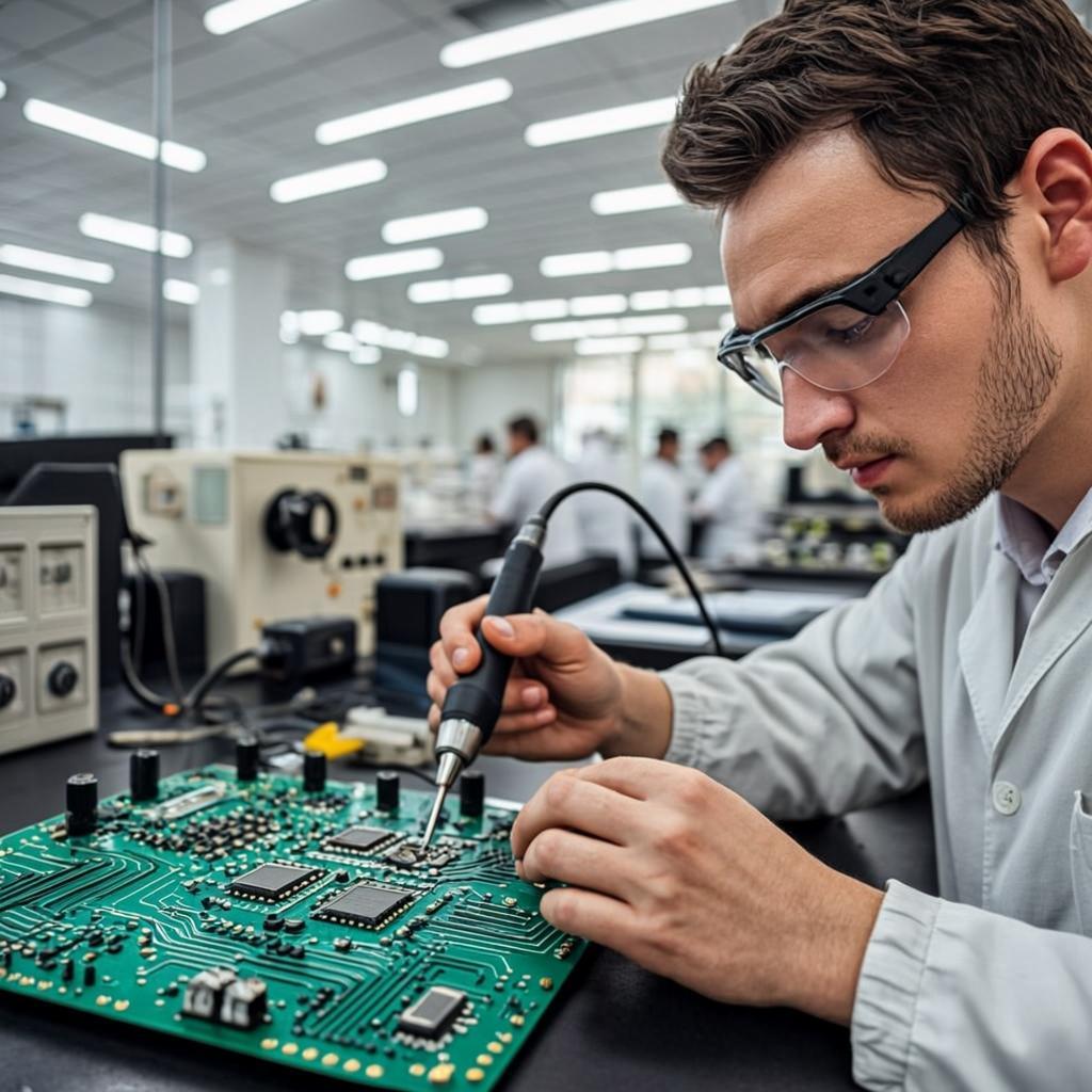
Close-up of a printed circuit board (PCB) under magnification, highlighting its intricate electronic components and soldering connections. The image represents the precision required in the PCBA (Printed Circuit Board Assembly) process.
After printing, conduct visual inspection and optical inspection (AOI) to verify the evenness and alignment of solder paste on all SMT pads. This stage sets the stage for flawless pick and place machine operations.
High-speed pick-and-place machines are used to accurately mount small electronic components. It is vital to ensure that the machine settings are correct and that the orientation and position of the components are accurate to avoid misplacement. Key points include:
This step is critical for ensuring precise placement of integrated circuits and passive components in SMT assembly.
Following high-speed placement, mid-to-low-speed machines handle larger or special-shaped components.
For general-purpose pick-and-place machines, they typically feature 3 to 5 placement heads, each capable of swapping 2 to 5 nozzles. These machines can place 1 to 2 components per second from tape reels and take 1 to 3 seconds for components from trays. This ensures complete component mounting before soldering. Generally, each SMT production line is equipped with one of these machines.
A pre-reflow visual inspection is conducted to identify misaligned, missing, loss, or improperly seated parts before the board enters the reflow oven.
Detailed view of a motherboard showing various electronic components and traces on a yellow PCB. This image demonstrates the complexity of PCB design and assembly for advanced electronics.
Reflow soldering is the core of SMT technology. It requires the appropriate temperature profile to be set. It is important to avoid overheating or poor cooling of solder joints to prevent defects.
The temperature profile is segmented into four key zones within the reflow oven: the preheat zone, thermal soak zone, reflow zone, and cooling zone. Each zone has specific temperature control requirements to ensure the quality of the solder joints and the reliability of electronic components.
When the PCB enters the preheat zone, the solvents and gases in the solder paste evaporate. At the same time, the flux in the solder paste begins to wet the pads, component terminals, and leads. The solder paste softens, collapses, and covers the pads, isolating them from oxygen.
As the PCB enters the thermal soak zone, it is preheated thoroughly to prevent damage to the PCB and components from a sudden rise in temperature when entering the reflow zone.
When the PCB reaches the reflow zone, the temperature rises rapidly, causing the solder paste to melt. The liquid solder wets, diffuses, and flows over the pads, component terminals, and leads, forming a solid solder joint.
Finally, the PCB enters the cooling zone, where the solder joints solidify, completing the reflow soldering process.
Maintaining an optimal profile is essential for reliable solder joints and overall PCB integrity.
Post-reflow, both manual inspection and automated optical inspection (AOI) systems are used to ensure solder joint quality and detect issues such as:
The solder joint appears visually acceptable but does not actually contact the component leads or pads. This defect may occur due to insufficient melting of the solder or inadequate wetting of the soldering area. Components with cold solder joints may fail to establish electrical connections, resulting in functional failure.
Excess solder appears between component leads, causing a short circuit.
The solder joint is not secure and may result from insufficient temperature or inadequate soldering time, leading to poor electrical contact.
Components may shift during the soldering process, resulting in incorrect positioning.
Small solder balls may form during the soldering process, posing a risk of short circuits.
Certain components may not be correctly placed or may be replaced with incorrect components.
The solder joint may be excessively large or small, or its shape may be irregular, potentially affecting electrical performance.
This occurs when the solder joint deviates from the intended form, potentially affecting electrical conductivity and mechanical strength, and can be caused by inconsistent solder paste application or improper soldering techniques.
Through-hole component (hole component) insertion requires precise alignment and depth control. Considerations during the DIP insertion process inlcude:
Before insertion, check the surfaces of electronic components for contaminants such as grease or paint. Ensuring that the surfaces are clean is crucial to avoid compromising the quality of insertion and soldering.
During the insertion process, ensure that the electronic components are flat against the PCB. After insertion, verify that the components are level and not uneven. Additionally, components with directional indicators must be inserted according to their specified orientation to prevent incorrect placement.
Ensure that the inserted leads do not obstruct the pads to guarantee the quality and reliability of soldering.
Be mindful of the force applied during insertion to avoid excessive pressure that could damage the components or the PCB.
When inserting electronic components, ensure they do not exceed the edges of the PCB, paying particular attention to the height of the components and the spacing between them.
a PCB with a mix of surface-mount and through-hole electronic components, including resistors, capacitors, ICs, LEDs, and connectors—demonstrating a typical PCBA layout used in electronic circuit design and assembly.
After DIP, a thorough visual inspection ensures that all through-hole solder joints are intact and aligned correctly for wave soldering, thereby guaranteeing product reliability.
Wave soldering involves passing the board over a wave of molten solder in a machine. This process is used for handling through-hole components, requiring appropriate soldering parameters to be set to ensure uniform soldering and to avoid cold solder joints. Detailed phases include:
Before wave soldering, the PCB must undergo cleaning and pre-treatment to remove surface oils, dust, and other contaminants, ensuring soldering quality.
Accurately place the DIP componen