WellPCB is a low loss PCB manufacturer delivering printed circuit boards that maintain signal integrity at high frequencies in demanding RF and microwave environments.
Our PCBs use premium low-loss materials such as Rogers, Isola, and Panasonic Megtron 6 laminates. These allow for low dielectric constants and low dissipation factors for improved signal.
WellPCB’s fabrication capabilities include precise impedance control, high frequency laminates and multi-layer stackups for complex circuit design.
Low loss printed circuit boards transmit high frequency signals with minimal attenuation. You’ll find them in applications like 5G base stations, satellite communications and automotive radar modules.
Engineered with premium frequency low loss PCB material, these boards maintain stable dielectric properties across a wide temperature range. They help support consistent impedance and low insertion loss for RF and microwave performance.
As a reliable low loss PCB manufacturer, we use high frequency laminates such as Rogers RO4350B, Isola Astra MT77 and Panasonic Megtron 6 (dielectric constants from 2.2 to 3.5 and dissipation factors down to 0.001). Copper weights range from 0.5 to 5 oz, with trace widths to 3 mil and impedance tolerances of ±5 Ω.
Fabrication integrates controlled lamination, laser-drilled microvias and precision etching to achieve extremely low transmission loss for high speed communication. Each PCB is tested using AOI, X-ray and impedance measurement to verify accuracy before shipment.
WellPCB’s low loss PCB manufacturing combines advanced high frequency laminates, precision impedance control and multi-layer stackup expertise.
We work with low loss PCB material grades including RO4003C and RO4350B, Isola 370HR and Isola 408HR,TU-883 and TU-768.
Dielectric constant values range from 2.2 to 3.5 with low dissipation factor down to 0.001, maintaining stable performance at high frequencies.
Laminates meet IPC and UL safety standards, with CTE values matched for low coefficient of thermal expansion in multi layer RF PCB builds.
Low loss PCBs are available from 1 to 64 layers, with HDI blind and buried microvias for compact high frequency PCB designs.
Our PCB stackup designs accommodate mixed dielectric materials to optimize impedance, insertion loss and skin effect performance for microwave PCB and high speed digital PCB layouts.
Finished copper thickness options from 0.5 oz to 5 oz, with plating tolerances of ±10% across the PCB board fabrication.
Heavy copper sections are available for power distribution layers in RF and microwave and radio frequency systems, while maintaining uniform plating thickness in fine-line areas.
We achieve impedance tolerances of ±5 Ω for single-ended and ±10% for differential pairs up to 110 GHz.
Vector network analyzer testing verifies S-parameters, insertion loss, and return loss, while design verification ensures impedance targets meet your design requirements.
Laser drilling supports microvias down to 0.1 mm diameter with ±0.05 mm positional accuracy. Through-holes maintain aspect ratios up to 25:1 with uniform copper plating.
We provide via-in-pad, stacked via, and via-in-via configurations to support high-density RF PCB and rigid-flex PCB layouts.
Our team can apply your choice of several surface finishes. These include ENIG (gold-plated nickel), immersion silver layers (0.12 to 0.40 μm), OSP coatings (0.2 to 0.5 μm) and lead-free HASL (from 1 to 40 μm).
Our team chooses each finish to minimize signal loss, maintain solderability and meet long-term reliability requirements for high frequency low loss PCB use.
Our facilities handle quantities from one-off PCB prototype builds to tens of thousands of units, with quick turn PCB lead times starting at 2 weeks for prototypes (up to 5 weeks for full production runs).
We apply statistical process control (SPC) to monitor plating thickness, hole quality and dimensions throughout the PCB manufacturing process.
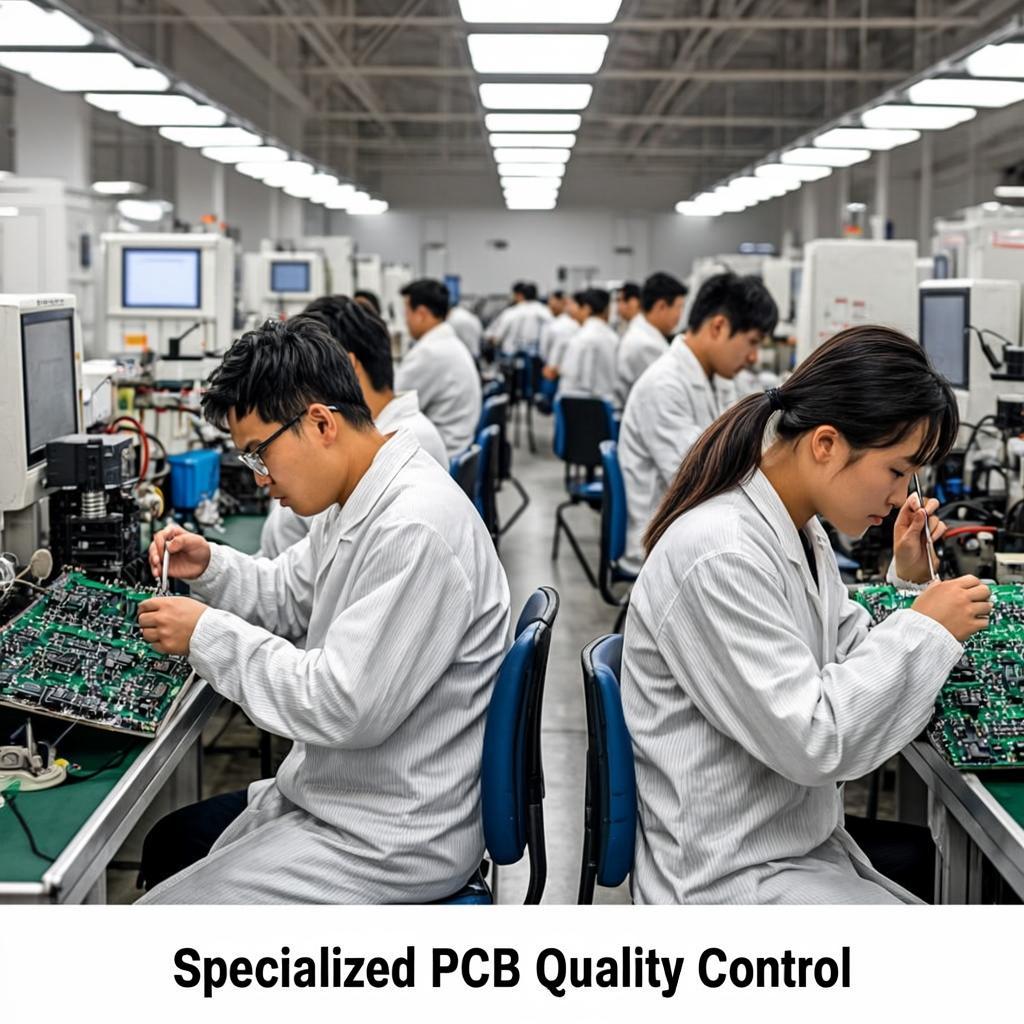
All low-loss PCB products undergo 100% AOI, flying probe or fixture-based electrical testing, X-ray inspection for internal structures and thermal cycling validation.
IPC Class 3 conformance and ISO 9001 certification ensure consistent quality in every batch, with assembly services available for complete fabrication and assembly delivery.
With over 18 years of PCB manufacturing experience, we produce low loss PCBs with controlled dielectric constant, low dissipation factor and precise impedance targets.
Our engineers maintain trace geometry, copper plating, and laminate handling to IPC Class 3 standards for consistent high performance.
We handle the full PCB manufacturing process, from laminate and prepreg materials selection through fabrication and assembly.
This includes substrate preparation, copper etching, impedance calibration, component sourcing and final PCB assembly. This helps us ensure uniform quality for every RF PCB and microwave PCB build.
Prototype low loss PCB orders can ship in as little as 3 weeks for RF and microwave projects. Standard runs complete in 4 to 5 weeks.
We support production from single PCB prototype quantities to 10,000+ unit volumes while maintaining the same performance.
Every low loss PCB undergoes impedance verification, AOI with 5 μm resolution, X-ray inspection and thermal cycling tests.
Electrical verification confirms insertion loss, signal integrity, and copper thickness using IPC-A-600 and IPC-TM-650 test methods to guarantee compliance with your design requirements.
We optimize material selection and PCB stackup to balance low transmission loss with budget constraints.
Hybrid constructions, controlled plating thickness and efficient panel utilization help reduce cost without compromising RF performance.
Our team conducts comprehensive design verification on all RF PCB and high frequency PCB projects.
We perform detailed checks to prevent redesign delays and ensure the final board matches your intended circuit design specifications.
A low loss PCB is a printed circuit board designed with low-loss materials to minimize dielectric loss and signal attenuation when used at high frequencies. Typical low loss PCB material includes RO4003C and RO4350B, Isola 370HR and Isola 408HR, TU-883 and TU-768. Fabrication integrates controlled impedance structures, smooth copper foils to reduce skin effect, and precision PCB stackup to meet insertion loss and return loss targets for high performance systems.
You’ll find low loss PCBs wherever high frequency signals, minimal signal loss and consistent impedance are necessary for the circuit to function. These boards are engineered to perform under strict electrical, thermal, and mechanical tolerances.
In 5G base stations, small cells and distributed antenna systems, low loss PCBs handle frequencies above 28 GHz with low insertion loss for stable, long-distance transmission.
Controlled impedance and low dielectric constant materials ensure consistent performance in massive MIMO and beamforming systems.
Advanced Driver Assistance Systems and radar sensors operating at 24 GHz and 77 GHz rely on low loss PCBs to maintain accuracy in detecing objects and lane assist functions.
High frequency laminates and low coefficient of thermal expansion materials withstand wide temperature swings in automotive environments.
MRI, CT and ultrasound systems use low loss PCBs to preserve signal clarity in high resolution imaging.
Low-loss materials reduce dielectric loss and EMI susceptibility, while maintaining a stable impedance during continuous operations.
Switches, routers and optical transceivers in data centers require low loss PCBs to meet signal integrity targets at 25 to 112 Gbps.
These boards maintain low transmission loss for high speed communication and reduce jitter in PAM4 signaling.
Smartphones, tablets and wearable devices with 5G, Wi-Fi 6E, and HDMI 2.1 connections benefit from low loss PCBs to ensure stable high frequency performance in compact rigid-flex PCB designs. These boards balance high density interconnects with efficient thermal management for reliable consumer use.
WellPCB sources and processes premium laminates that balance low dielectric constant, low dissipation factor, and mechanical stability, ensuring optimal performance for RF, microwave, and high speed digital applications.
PTFE laminates, such as Taconic and Rogers RT/duroid, deliver dielectric constants between 2.1 and 2.6 with dissipation factors as low as 0.0009.
These materials work well for RF and microwave PCB designs above 20 GHz, offering minimal signal loss and stable performance in high frequency low loss PCB applications.
Rogers RO4003C and RO4350B are part of the RO4000 series, designed to deliver stable dielectric constants (3.38 for RO4003C and 3.48 for RO4350B) across wide temperature ranges with low dissipation factors down to 0.0027.
These laminates are widely used in 5G, radar, and satellite systems, offering consistent impedance control and low insertion loss for high speed digital and RF circuits.