If you’re working on high-density electronics requiring serious signal integrity, a 20 layer PCB is likely on your radar. After spending 15+ years designing complex circuit boards for aerospace and telecom clients, I can tell you that moving from 8 or 12 layers to 20 brings both tremendous capabilities and unique challenges. This guide covers everything you need to know about 20 layer PCB design, stackup configuration, manufacturing processes, and real-world applications.
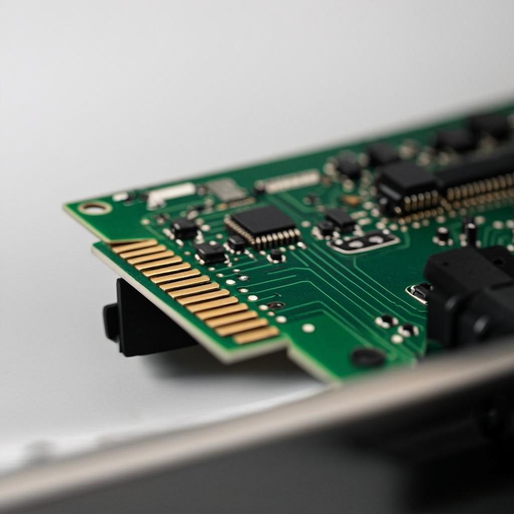
A 20 layer PCB is a high-density multilayer printed circuit board containing twenty conductive copper layers separated by insulating dielectric materials. These boards use alternating layers of copper foil, prepreg (pre-impregnated fiberglass), and FR-4 cores bonded together through sequential lamination.
Each copper layer serves a specific function in the design. Signal layers carry high-speed data traces, while dedicated ground and power planes provide stable reference voltages and return paths for electrical signals. The careful arrangement of these layers directly impacts signal integrity, electromagnetic compatibility, and overall board performance.
Most 20 layer boards measure between 2.4mm and 6.6mm in total thickness, depending on the dielectric materials and copper weights used. Standard builds with 1oz copper and typical FR-4 dielectrics usually come in around 4.3mm to 5.3mm thick.
Layer Assignment (10 Signal + 5 GND + 5 PWR)
20L Targets
Impedance
Power Integrity
Applications
The primary reasons engineers specify 20 layer boards include:
Getting your stackup right determines whether your 20 layer PCB succeeds or fails. I’ve seen too many designs fall apart because someone threw layers together without considering impedance, coupling, or manufacturability.
A well-designed stackup alternates signal layers with ground and power planes in a balanced, symmetrical configuration. This symmetry prevents warping during thermal cycling and ensures consistent electrical performance across the board.
Here’s what a typical 20 layer stackup looks like:
When designing your 20 layer PCB stackup, follow these principles:
Read more PCB layers:
The dielectric materials you choose affect everything from signal speed to thermal performance:
For most 20 layer designs running signals under 5Gbps, standard FR-4 works fine. Once you push into 10Gbps territory, materials like Megtron 6 or similar low-loss laminates become necessary to maintain signal integrity.
Controlled impedance is critical for 20 layer PCBs carrying high-speed signals. The impedance of a transmission line depends on trace width, dielectric thickness, dielectric constant, and copper thickness.
Common Impedance Targets
Achieving tight impedance control requires collaboration with your manufacturer. They’ll calculate trace widths based on actual material properties and provide a controlled impedance report with delivered boards.
Impedance Calculation Considerations
The dielectric constant (Dk) of laminate materials varies with frequency. A material specified at Dk=4.2 at 1MHz might measure Dk=3.8 at 10GHz. For high-frequency designs, use frequency