Taconic RF-60A is a specialized PTFE-based PCB material designed to meet the needs of high-frequency applications, including RF and microwave systems. Known for its exceptional electrical performance and stability, RF-60A offers low signal loss and consistent performance across a range of demanding environments. This material excels in applications such as 5G base stations, satellite communication, automotive radar, and IoT devices. Through its precise dimensional control, superior laminate properties, and compatibility with various surface finishes and stack-ups, RF-60A ensures optimal performance in even the most challenging conditions. In the following sections, we’ll break down the key features, manufacturing techniques, and design considerations that make Taconic RF-60A an excellent choice for high-frequency circuit designs.
Designing RF and microwave PCBs isn’t just about copper thickness or trace width—it starts at the core: the laminate. Taconic RF-60A PCB materials are engineered for RF circuit structures that operate in the GHz range, offering dependable electrical behavior, stable performance under heat, and low loss. These materials are favored in applications like aerospace radar systems, 5G communication hardware, and RF power amplifiers, where signal degradation just isn’t an option.
RF-60A’s PTFE-ceramic blend sets it apart in applications that demand tight impedance control, low insertion loss, and high reliability in humid or high-temp conditions. The material offers not only measurable stability but also production consistency, which helps us maintain quality across multiple production runs.
Taconic RF-60A PCB laminates are made with ceramic-filled polytetrafluoroethylene (PTFE) and reinforced fiberglass cloth. This structure ensures solid electrical integrity and dimensional predictability, even when subjected to reflow temperatures or multilayer lamination.
What this means for your project:
For microwave engineers and PCB designers, dielectric performance drives nearly every decision in the signal layer stackup. Taconic RF-60A PCB materials offer tight control over dielectric properties across both sheet and batch production. This means you can route RF lines and microstrip structures without running into inconsistent impedance or phase delay shifts.
Performance benefits:
PTFE-based laminates are known for moisture resistance, but Taconic RF-60A PCB laminates take it a step further with optimized filler ratios and tight process control. This helps reduce dielectric drift in humid environments and allows reliable adhesion during reflow or lamination.
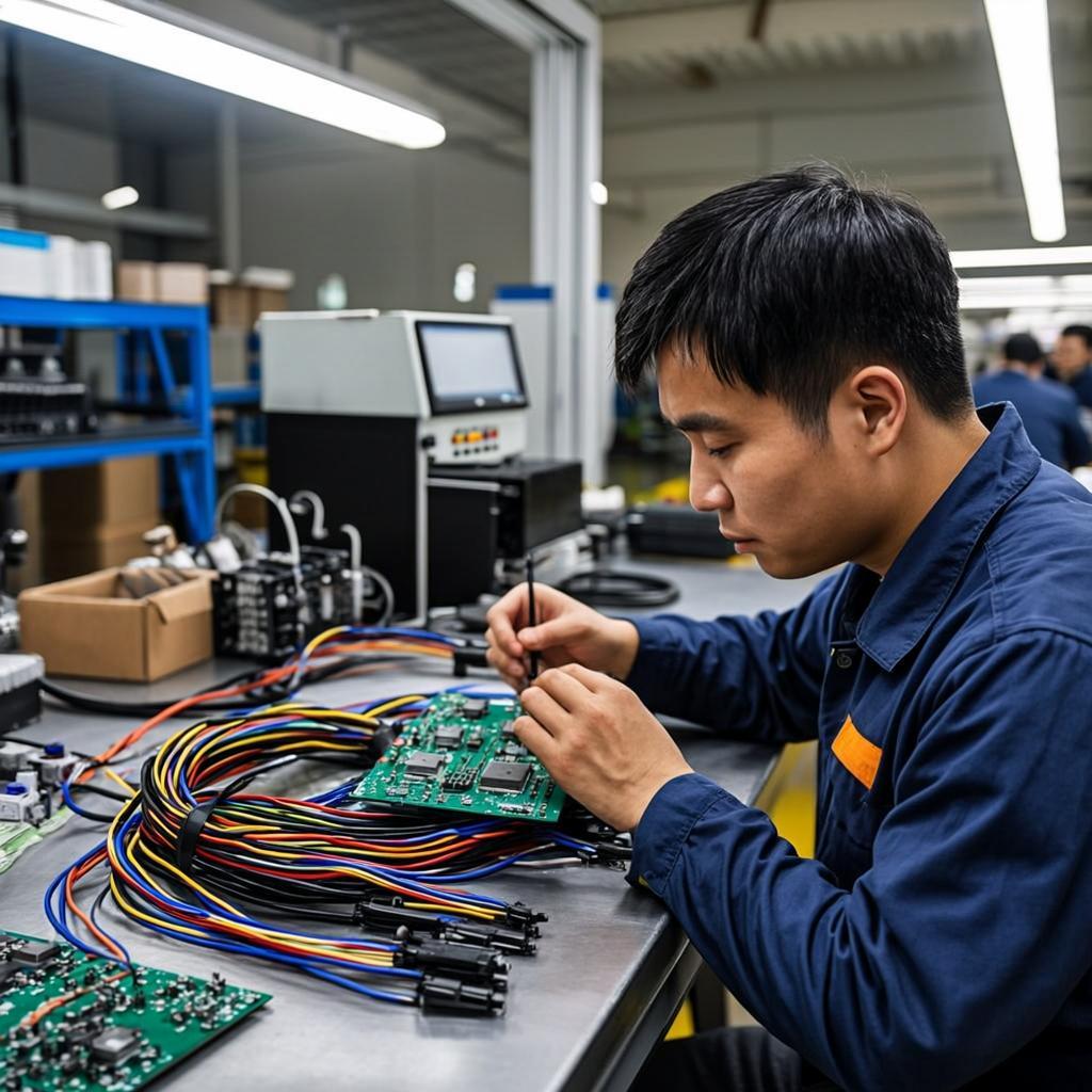
Here’s what that looks like on the shop floor:
Pro tip: When dealing with high-layer count boards, RF-60A’s low in-plane expansion helps prevent misregistration and drill breakout.
Taconic RF-60A PCB Materials
Designing high-frequency PCBs requires a detailed approach to materials, stack-up, and layout to ensure optimal performance. Taconic RF-60A, known for its low loss and consistent dielectric properties, offers a stable foundation for RF and microwave circuits. This section addresses best practices for controlling impedance, planning stack-ups, and laying out circuits to minimize signal reflection and optimize transmission.
In high-frequency layouts, maintaining controlled impedance supports consistent signal transmission. Taconic RF-60A provides a stable dielectric constant (Dk) of 6.15 ±0.25 at 10 GHz, which minimizes signal loss and ensures predictable behavior in high-frequency applications.
To achieve controlled impedance, we need to calculate trace widths based on the target impedance (typically 50Ω for single-ended traces and 100Ω for differential pairs) and the Dk of the material. Taconic RF-60A’s stable Dk reduces the chances of impedance mismatches, preventing signal degradation or reflections.
The use of vias should be minimized since they can cause impedance discontinuities. Carefully placed vias help maintain stable return paths, but overuse can introduce unwanted resistance and inductance that may affect signal quality. A solid ground plane beneath the signal layers is also recommended for maintaining a consistent return path.
Stack-up design influences signal control and helps limit electromagnetic interference. A typical approach when using Taconic RF-60A is to employ a multi-layer stack-up that includes dedicated ground and power planes between signal layers. This arrangement reduces noise and crosstalk, while helping to maintain consistent impedance across the layers.
By carefully positioning ground and power planes adjacent to signal layers, the signal quality is preserved. For example, a 4-layer stack-up could use outer signal layers, with internal power and ground planes to shield the signals and reduce interference.
For more complex designs, a 6-layer stack-up can provide additional isolation. This layout balances signal and power layers while also contributing to reduced electromagnetic interference (EMI), leading to better overall performance.
Achieving low return loss is a primary goal in RF layouts, as it reduces signal reflection and ensures signals travel smoothly through the PCB. Several layout best practices can help achieve this goal:
By applying these layout techniques, we can reduce reflections, achieve low return loss, and enhance signal performance in high-frequency applications.
Taconic RF-60A PCB Manufacturing
The manufacturing of Taconic RF-60A PCBs involves an intricate set of processes designed to maintain the integrity of high-frequency signals. These processes, from drilling and routing to surface finish selection and dimensional control, contribute to the overall performance of RF circuit boards. In this section, we dive deeper into these fabrication techniques, detailing how each step enhances the final product for use in RF and microwave applications.
Manufacturing Taconic RF-60A PCBs involves specialized techniques for drilling, routing, and via preparation, which are all tailored to the needs of high-frequency designs. These processes ensure that the structure of the PCB remains stable and effective in supporting RF signals.
For RF-60A boards, precise drilling is needed to achieve clean and well-formed vias. This precision helps maintain the structural integrity of the PCB and limits parasitic effects that can disrupt signal transmission. CNC drilling systems ensure that vias are cleanly formed with minimal deviation, preventing defects that could impair performance in high-frequency designs.
When working with Taconic RF-60A materials, preparing vias is especially challenging due to the unique PTFE-based composition of the substrates. This composition can make traditional drilling methods less effective, so advanced methods such as laser drilling or mechanical drilling are often employed. This preparation ensures that vias are smooth and well-formed, minimizing the risk of poor copper plating that could affect signal quality.
For more complex designs, such as those requiring buried or blind vias, we must be precise in their alignment to ensure that no disruptions to the signal path occur. Every aspect of via preparation is closely controlled, from hole diameter to pad and trace dimensions, helping to ensure that the PCB remains well-suited to the high-frequency environment.
The choice of surface finish affects both the service life and electrical behavior of Taconic RF-60A PCBs, especially in terms of solder joint quality and high-frequency signal performance. Options such as ENIG, immersion tin, and gold plating each offer distinct characteristics that may be selected based on soldering method, environmental exposure, and frequency range.
ENIG is a widely used surface finish for Taconic RF-60A PCBs, providing good corrosion resistance and solderability. The gold layer creates a smooth and flat surface that is ideal for soldering, while the nickel layer underneath offers added stability and durability. This finish also minimizes the potential for signal loss and reduces the risk of oxidation over time, making it a suitable choice for high-frequency applications.
Another surface finish option is immersion tin, which is known for its cost-effectiveness and solderability. While immersion tin is a simpler finish than ENIG, it still delivers reliable performance in many RF applications. The flatness it provides is adequate for many designs, though it may not offer the same performance benefits at very high frequencies compared to more robust finishes like ENIG.
Gold plating is often selected for RF-60A PCBs when extra durability is needed. Gold offers superior resistance to oxidation and corrosion, providing long-lasting protection in demanding environments. In high-frequency applications where reliability is a top concern, gold plating ensures that the PCB maintains its quality over time, even in harsh conditions.
Maintaining dimensional accuracy and stability is a core aspect of the Taconic RF-60A PCB manufacturing process. High-frequency applications demand precise control over the size and shape of each layer and via, as even slight variations can affect signal integrity.
Multilayer PCBs require careful alignment to ensure that all copper layers are properly positioned. Any misalignment can lead to trace width or spacing issues, which can introduce impedance mismatches and signal degradation. Automated optical inspection (AOI) systems are used to monitor and correct any misalignment during the lamination process, ensuring.