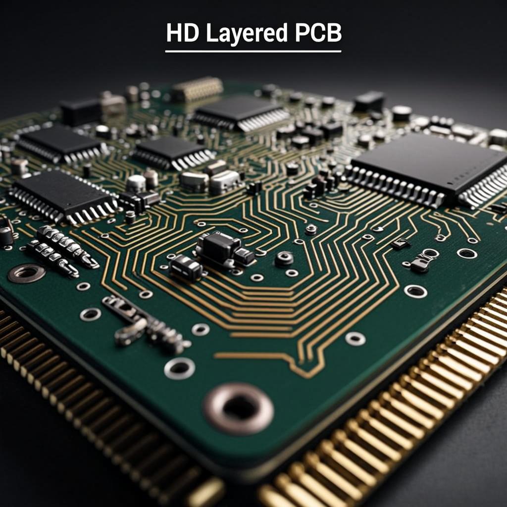
Compared to the traditional single-layer PCB, multilayer PCBs consist of 3 or over 3 layers of conductive copper foils. A Double-Sided PCB has two conductive layers on top and bottom of the PCB substrate. The top and bottom layers of a multilayer PCB look like that of a double-sided PCB but there are more layers on both sides of the core. They often appear as Many layers of double-sided circuit board glued and laminated together with layers of heat-protective insulations. Copper-plated holes interconnect these layers, and electric connections from the middle of the layers are obtained from vias such as blind and buried vias, plating through holes.
On the top and bottom layers of the multilayer PCB, there are active and passive components placed while the inner stacked layers are used for routing. It is arranged so that on the PCB, two layers are placed on the surface to connect the environment. Both through-hole electronic components and Surface Mount Components (SMD)can be soldered on either side of this type of PCB. SMD components can be soldered with Surface Mount Technology and other PCBA Tools. By applying such methods, producers can construct different sizes of highly complex PCBs.There can be up to 40 layers for multilayer PCBs.
Single-layer boards, also known as single-sided PCB have just one layer of base material, also known as a PCB substrate.
Double-sided PCBs or double-layer printed circuit boards, as the name suggests, are more complicated than Single Sided PCBs as they consist of one single layer of the base substrate with 2 conductive (copper) layers on both sides of the substrate. There are solder masks applied on both sides of the board as well.
The definition of a multilayer PCB is a PCB that is made with three or more conductive copper foil layers. Once you look closer at the three primary types of PCB boards, you'll see there are many other differences in how they're constructed and how they function.
Single-layer boards, sometimes called single-sided boards, have components on one side of the board and a conductor pattern on the opposite side. They have just one layer of conductive material, typically copper. A single-layer board is comprised of a substrate layer, a conductive metal layer, and then a protective solder mask and silk screen. You'll find single-layer boards in many simpler electronic devices.
You can also use a double-layer or double-sided board, which has more layers than a single-layer board but fewer than a multi-layer. Double-sided PCBs, like the single-sided variation, have one substrate layer. The difference is that they have a layer of conductive metal on both sides of the substrate.
Circuits and components on one side of the board are connected to those on the other side through one of two methods:
Multi-layer PCBs are made of three or more double-sided boards stacked on top of each other. Theoretically, they can contain as many boards as you can need, but the largest one ever made was 129 layers thick. Typically, they have an even number of between four and 12 layers — odd amounts can cause problems such as warping and twisting post-soldering.
Each substrate layer in a multi-layer board has a conductive metal on both sides of it. The boards are joined together using a specialized kind of adhesive, and there is an insulating material between each board. On the very outer edges of the multi-layer board, you'll find solder masks.
Multi-layer boards typically appear in more complex devices that require a high number of connections.
Paths known as vias allow the different layers to conduct to each other. These paths fall into three groups: Through-Hole, Blind via, and Buried via, see more details about them below.
To put it simply, via refers to an electrical connection between different layers on the printed circuit board. Vias come in three types: through-hole vias, blind vias, and buried vias.
Through-hole vias also known as standard vias pass through all layers of the printed circuit board to connect the top, bottom, and inner layers. Their dimensions are larger than those of other via types, and drilling is not restricted.
The blind vias are typically drilled from the outside layer of the printed circuit board to the inner layers without making a hole on the other side of the board. For the holes cannot be seen from another side of the board, they are referred to as ‘’blind” vias.
Buried vias connect two or more inner layers of the printed circuit board and are not visible on either outer layer. In the production of multilayer PCBs, the internal plating of the buried vias must be completed before applying the two outer layers of the board. As they require to be designed more precisely, the Manufacturing cost will increase for buried vias.
For there are more chances of cross connections, overlaps, tracing in copper areas, etc. It’s detailed and patience-needing work to produce multilayer PCBs and the whole manufacturing process requires special precaution. The whole process needs to be finished in an SD(electrostatic discharge)-Safe and Cleanroom environment. Special manufacturing setup and equipment are needed for the 8+ layer PCB manufacturing process.
Here are the basic steps involved in Multilayer PCB Manufacturing Process:
Design-The process starts with designing the Layout of the PCB using any PCB designing software / CAD Tool (Proteus,Eagle,OrCAD).
Making the Inner Layer Core- Laminate of desired thickness is treated with Copper foil, dry film resistance, and UV light to make the inner layer core.
The lamination- This process includes the Inner layer core, prepeg sheets, and copper foil sheets. The sheets of material are staked on each other and holes are used to align them as they are stacked up.
For a 4-layer board, the Staking of layers is as follows: Bottom Layer of Copper Foil – Prepeg Sheets – The Inner Layer Core – More Prepeg Sheets – Finally Copper Foil Sheet on Top.
Applying pressure- heat and vacuum using a heated hydraulic press. The vacuum is important to make sure there is no air trapped between the layers. This process ends over 2 hours depending on the number of layers.
Forming- Once cured, resins from the prepegs join the sheets, core, and foil together forming a multilayer PCB.
See the tech and processings applied in multilayer PCB production here:
Cutting-The process of cutting the original copper-clad board into a board that can be made on the production line.
Inner Dry Film-The inner dry film is the process of transferring the inner circuit pattern to the PCB board.
Black Oxidation-The boards with inner layer wiring must be blackened or browned before they can be laminated. It is to oxidize the copper surface of the inner layer board. It is used to add mild corrosion resistance, for appearance, and to minimize light reflection.
Lamination-Lamination is the process of bonding layers of circuits into a whole using B-stage prepreg.
Mechanical Drilling-Mechanical drilling is to use a drill to cut at high speed to form a through hole in the PCB.
Metalize The Through Hole-The metallization of the hole is to solve the problem of covering the cross-section with a uniform, thermal shock-resistant metal copper.
Dry Film & Pattern Plating- The outer layer graphics transfer is similar in principle to the inner layer graphics transfer. Both use photosensitive dry film and photographic methods to print circuit patterns on the board.
Solder Mask-The solder mask process is to add a layer of solder mask on the surface of the board for protection against oxidation and to prevent solder bridges from forming between closely spaced solder pads.
The specific process is as follows: Pre-treatment-> coating one> pre-bake-> exposure-> development-> UV curing-> thermal curing.
Silkscreen- Silkscreen is a layer of ink traces used to identify components, test points, parts of the PCB, warning symbols, logos, marks, etc.
Surface Finished-The most basic purpose of surface treatment is to ensure good solderability or electrical properties.
Profiling-The process of PCB profile is to cut PCBs from a working panel to be set or individual Pcs according to the customer's requirement, normally there are three types of PCB profile in the PCB manufacturing process, the most popular one is milling, also known as routing, the second one is V-Cut, and the third one is punch.
E-TEST-The electronic test is the electrical performance test of the PCB, which is usually also called the "on" and "off" test of the PCB.
Final inspection-Inspection methods usually include Optical inspection, target inspection confirmation, and visual inspection confirmation to confirm or eliminate some true and false defects.
Package- The main packaging types are Anti-Static Packaging, Moisture-Proof Packaging, and Anti-Vibration Packaging, but the usual packaging only uses vacuum packaging.
These merits make multilayer PCBs excel, with so many industries stepping into mobile solutions, multilayer PCBs are taking a really significant role in many industry-specific applications.